Surface preparation prior to deposition

a surface preparation and film technology, applied in the direction of coatings, chemical vapor deposition coatings, semiconductor devices, etc., can solve the problems of increased manufacturing costs, lower throughput, and slow nucleation, and achieve the effect of convenient subsequent deposition, low cost, and rapid nucleation

Inactive Publication Date: 2006-06-06
ASM IP HLDG BV
View PDF32 Cites 15 Cited by
  • Summary
  • Abstract
  • Description
  • Claims
  • Application Information

AI Technical Summary

Benefits of technology

[0019]Prior to depositing, the preferred embodiments treat the surface with plasma products. Advantageously, CVD polysilicon and poly-SiGe more readily nucleates over the treated surface, or ALD reactants more readily adsorb upon the treated surface. The surface treatment provides surface moieties more readily susceptible to a subsequent deposition reaction, or more readily susceptible to further surface treatment prior to deposition. By changing the surface termination of the substrate with a low temperature radical treatment, subsequent deposition is advantageously facilitated without depositing a layer of any appreciable thickness and without significantly affecting the bulk properties of the underlying material.

Problems solved by technology

Slow nucleation entails higher overall deposition times, lower throughput and consequently greater fabrication costs.
The semiconductor industry is very sensitive to fabrication costs.
Accordingly, any increase in wafer throughput, at any stage of processing, translates to reduced production costs and higher margins.
Furthermore, the initial poor nucleation can lead to poor quality of the resultant layer, including problems with stoichiometry, density, surface planarity, etc.
However, this additional step complicates the process flow and requires adjustment of the doping concentrations at the dielectric-electrode interface to ensure the desired work function for the transistor.
Ultra thin gate oxides (e.g., less than 5 nm), however, have been found to exhibit high defect densities, including pinholes, charge trapping states, and susceptibility to hot carrier injection effects.
Such high defect densities lead to leakage currents through the gate dielectric and rapid device breakdown unacceptable for circuit designs with less than 0.25 μm gate spacing, i.e., sub-quarter-micron technology.
While care under laboratory conditions can be used to control defect densities, such control has been difficult to achieve under commercial volume fabrication conditions.
Moreover, even if the integrity of the oxide is perfectly maintained, quantum-mechanical effects set fundamental limits on the scaling of gate oxide.
As noted above, it is often difficult to deposit electrode materials, such as polysilicon, amorphous silicon, and particularly doped silicon or silicon germanium alloys, over conventional silicon oxides as well as many of the high k materials currently under investigation.
Many other types of materials and deposition techniques in integrated circuit fabrication face issues that depend upon the substrate surface upon which the material is to be deposited.
Such intermediate layers add to the complexity and cost of fabrication, and can also occupy valuable space within high aspect ratio features, such as contact vias or folded structures for high surface area capacitors.
In some contexts, like gate dielectrics and capacitor dielectrics, additional layers increase the overall dielectric thickness and reduce the effectiveness of the layer, contrary to the trend for scaling down integrated circuits.

Method used


Image

  • Surface preparation prior to deposition
  • Surface preparation prior to deposition
  • Surface preparation prior to deposition

Examples


Embodiment Construction

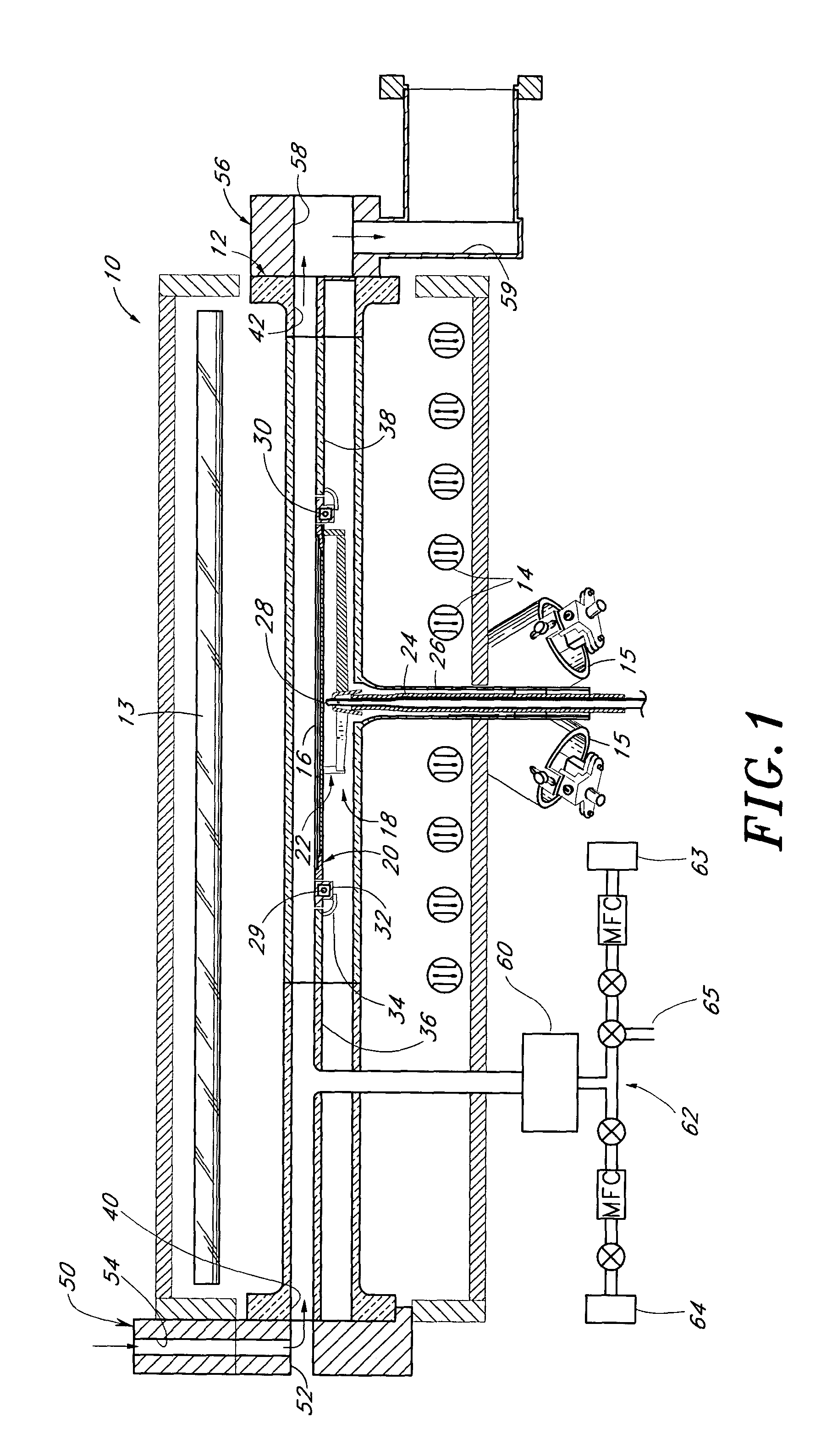
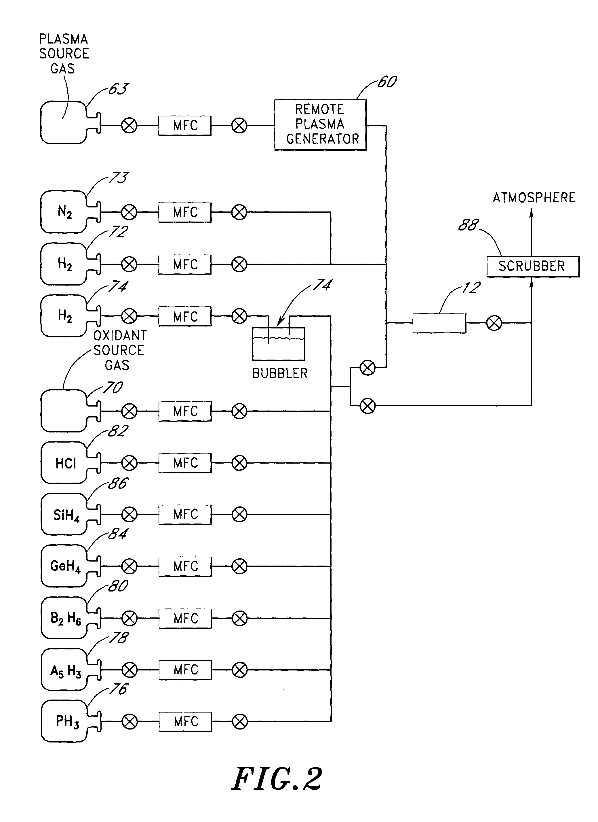
[0027]The skilled artisan will readily appreciate that the principles disclosed herein will have application to a variety of contexts in which interface preparation prior to deposition is desired. Such preparation is particularly advantageous for nucleation-sensitive and adsorption-driven processes.

[0028]In accordance with the preferred embodiments, the invention provides treatment of surfaces with plasma products prior to deposition. The plasma products preferably modify surface termination to make them susceptible to subsequent deposition

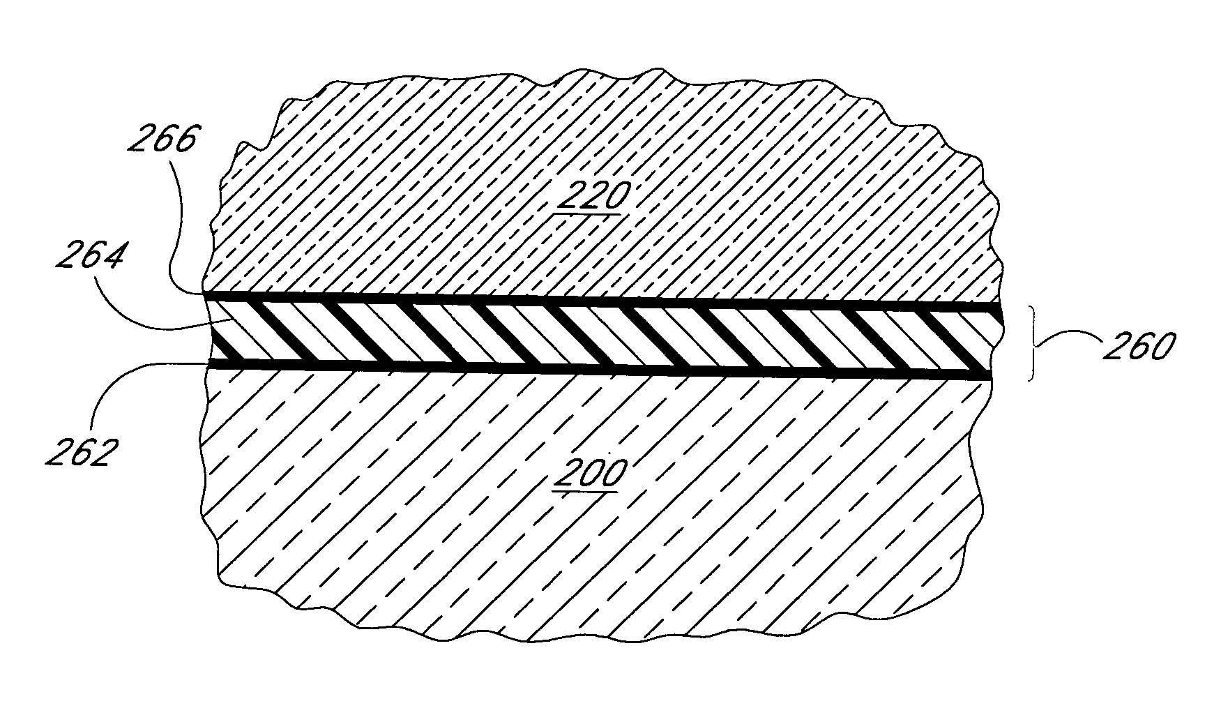
[0029]As noted in the Background section above, many deposition processes are sensitive to the surface over which deposition is required. Doped polysilicon and polycrystalline silicon-germanium alloy (poly-SiGe) tend to nucleate poorly over silicon oxide, as is well known in the art, and also over newer high-k materials now being investigated. The present invention provides a method for preparing the dielectric surface for electrode deposition the...


PUM

PropertyMeasurementUnit
total volume capacityaaaaaaaaaa
total volumeaaaaaaaaaa

Abstract

Methods are provided herein for treating substrate surfaces in preparation for subsequent nucleation-sensitive depositions (e.g., polysilicon or poly-SiGe) and adsorption-driven deposition (e.g. atomic layer deposition or ALD). Prior to depositing, the surface is treated with non-depositing plasma products. The treated surface more readily nucleates polysilicon and poly-SiGe (such as for a gate electrode), or more readily adsorbs ALD reactants (such as for a gate dielectric). The surface treatment provides surface moieties more readily susceptible to a subsequent deposition reaction, or more readily susceptible to further surface treatment prior to deposition. By changing the surface termination of the substrate with a low temperature radical treatment, subsequent deposition is advantageously facilitated without depositing a layer of any appreciable thickness and without significantly affecting the bulk properties of the underlying material. Preferably less than 10 Å of the bulk material incorporates the excited species, which can include fluorine, chlorine and particularly nitrogen excited species.

Description

REFERENCE TO RELATED APPLICATION[0001]This application is a continuation of U.S. patent application Ser. No. 09 / 944,734 (filed 31 Aug. 2001), now U.S. Pat. No. 6,613,695 which claims the benefit of U.S. Provisional Applications 60 / 253,693 (filed 24 Nov. 2000) and 60 / 283,584 (filed 13 Apr. 2001).FIELD OF THE INVENTION[0002]The invention relates generally to surface preparation prior to film deposition for semiconductor fabrication, and are particularly to surface preparation to facilitate adsorption in subsequent atomic layer deposition (ALD) processes, or to facilitate nucleation of subsequent chemical vapor deposition processes.BACKGROUND OF THE INVENTION[0003]Integrated circuit design is constantly being scaled down in pursuit of faster circuit operation and lower power consumption. Scaled dimensions in a circuit design generally requires attendant changes in fabrication processing.[0004]A basic building block of integrated circuits is the thin film transistor (TFT). As is known i...

Claims


Application Information

Patent Timeline
Patent Type & Authority Patents(United States)
IPC IPC(8): H01L21/31C23C16/42C23C16/02C23C16/22C23C16/40C23C16/44C23C16/455H01L21/205H01L21/28H01L21/306H01L21/3105H01L21/316H01L21/3205H01L29/51
CPCC23C16/0218C23C16/22C23C16/403C23C16/405C23C16/45525C23C16/56H01L21/02178H01L21/02189H01L21/0228H01L21/02315H01L21/28017H01L21/28035H01L21/2807H01L21/28185H01L21/28194H01L21/28202H01L21/306H01L21/3105H01L21/3141H01L21/31604H01L21/3162H01L21/32055H01L29/513C23C16/0245H01L29/518H01L29/517H01L21/203
Inventor POMAREDE, CHRISTOPHE F.ROBERTS, JEFFSHERO, ERIC J.
Owner ASM IP HLDG BV
Why Eureka
Try Eureka