
System for cushioning wafer in wafer carrier

Inactive Publication Date: 2006-06-13
ENTEGRIS INC
View PDF19 Cites 30 Cited by
  • Summary
  • Abstract
  • Description
  • Claims
  • Application Information

AI Technical Summary

Benefits of technology

[0009]The wafer transport system of the invention provides wafer carriers that solve these long-felt problems by providing adequate damage protection and particulate protection with minimal contamination of the wafers in the shipper. Part of the solution to these problems involved recognizing that a material suitable for use as a wafer carrier should have inherent static-control properties as opposed to being treated for static control. Treatments involve adding substances to the material that are readily separated from the material. In contrast, a material with inherent static control has more stability and resistance to degassing or throwing off particulates.
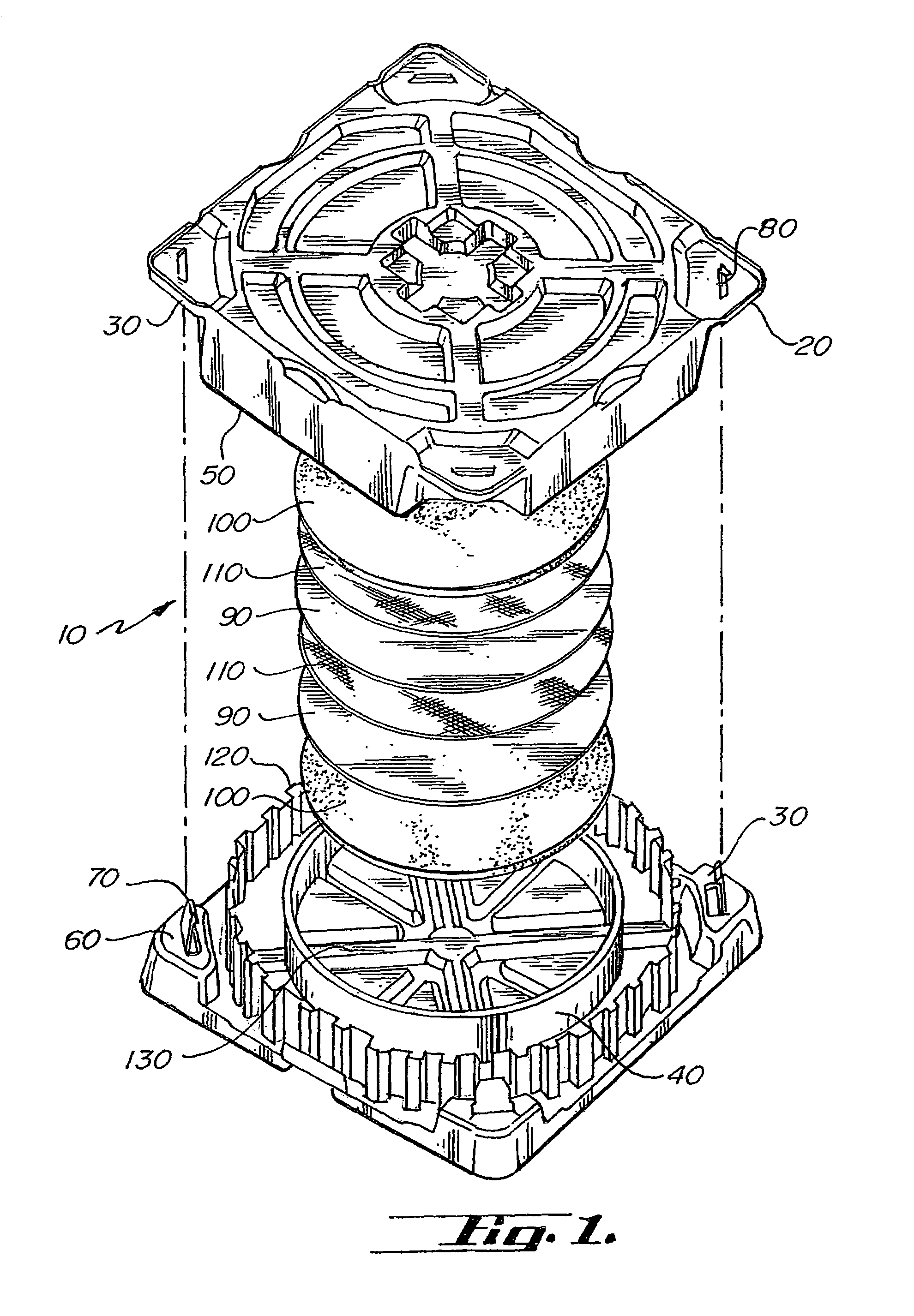
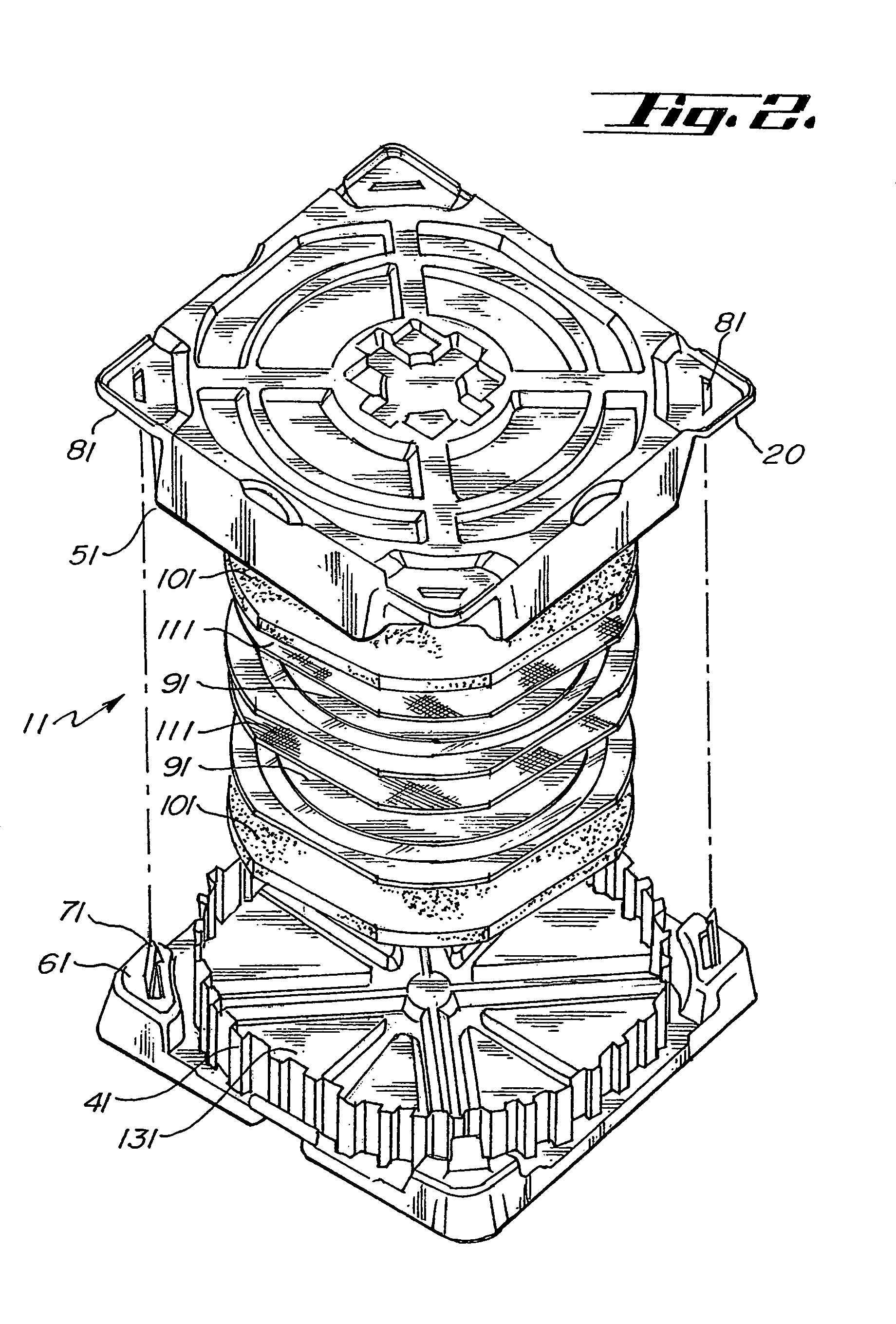
[0012]An embodiment of the system has a wafer carrier base, at least one wafer lateral support, a wafer carrier cover, and at least one wafer cushion. The base and wafer lateral support cooperate to define a wafer stack pocket that the semiconductor wafers can be stacked in. The wafer faces are approximately perpendicular to the lateral support so that the wafers can be transported in a horizontal position. The wafer carrier cover cooperates with the carrier base to traverse the wafer stack pocket and protect it from damage, shocks and particulates. The wafer cushion fits into the wafer stack pocket and has a layer of material that is 2 to 10 mm thick that is made of an energy-absorbing, closed-cell polyethylene foam material having a density of 1.5 to 1.9 pcf, a surface resistivity of less than 5×10⁷ ohms per square, and less than 1800 ng / g Cl−, 400 ng / g F− / Acetate, 270 ng / g NO3−, 350 ng / g SO42−, and 60 ng / g PO43−ions leachable under moderate conditions. The cushion preferably has no detectable outgassing organics as measured under stringent conditions. The static control properties are preferably the result of carbon that is part of the structure of the material.

Problems solved by technology

As semiconductors have become larger in scale, that is, as the number of circuits per unit area has increased, contaminants in the form of particulates have become more of an issue.
Chemical species that coat the wafers can interfere with subsequent processing steps.
Charged ions and amines are especially undesirable contaminants.
These cushions, however, outgas ions, amines, and other chemical species that contaminate the wafers.

Method used


Image

  • System for cushioning wafer in wafer carrier
  • System for cushioning wafer in wafer carrier
  • System for cushioning wafer in wafer carrier

Examples


example 1

Procedures for Testing for Ion Release Under Moderate Conditions

[0027]This example details the testing for ion release under moderate conditions. The method leaches materials with ultra-pure DI water for anion and cation analysis by ion chromatography.

[0028]The tests were performed using: Re-pipetter (RAININ) and corresponding tips or equivalent; Class 100 Laminar Flow Hood; PRECISION 180 Series Hot Water Bath or equivalent; Lead Ring Weights; 125-ml Polypropylene (PP) sample bottles; 18-MW / cm deionized water; 1000 ppm standards of fluoride, acetate, formate, chloride, nitrite, bromide, nitrate, sulfate, phthalate, phosphate, lithium, ammonium, sodium, potassium, magnesium, and calcium. “ppb” is defined as one nanogram per milliliter, (μg / ml); “ppm” is defined as one microgram per milliliter, (μg / ml). Clean class 10 nitrile gloves are worn while performing this procedure and as much sample preparation as was reasonably possible was performed in the class 100 laminar flow hood. All d...

example 2

Results of Testing for Ion Release Under Moderate Conditions

[0031]The procedures of example 1 were followed while analyzing multiple materials, including the following four materials: closed cell static-controlled polyethylene (PLASTAZOTE from ZOTEFOAM incorporated, Surrey, England); open cell anti-static polyurethane; corrugated conductive anti-static closed cell cross-linked high density crosslinked polyethylene; and closed cell anti-static polyethylene (CELLUPLANK). The results are tabulated in Table 1. Significantly, only one material provided less than 1800 ng / g Cl−, 400 ng / g F− / Acetate, 270 ng / g NO3−, 350 ng / g SO42−, and 60 ng / g PO43− ions leachable under moderate conditions.

[0032]

TABLE 1Results for Foam TestingHighLeachedClosed cellOpendensityClosed cellIonspolyethylenecellpoly-polyethyleneng / gPLASTAZOTEpolyurethaneethyleneCELLUPLANKCl−1600200042007200F- / Acetate220850150097000NO3−210220280approx 2500SO42−300370370approx 2500PO43−11050000OutgassedAminesAmines presentorganicspr...

example 3

Organic Outgassing Analysis by Gas-Chromatography-Mass Spectrometry

[0033]This example details procedures for measuring organic outgassing under stringent conditions. The method uses an automated thermal desorbtion unit (ATD) and analyzed via gas-chromatography-mass spectrometry (GC-MS). See also Thermal Desorbtion Gas Chromatograph, FGTM 1350. The following materials are required: Automatic Thermal Desorbtion Unit; Thermal Desorbtion Sample Tubes (glass); Thermal Desorbtion Sample Tubes (stainless steel) (SUPELCO P / N 255055); Thermal Desorbtion Sample Tubes (glass) (SUPELCO P / N 25090-U); 500 ppm heptane in methanol certified standard Gasoline Range Organic Standard. The following definitions apply: ppb is one nanogram per milliliter, (ng / ml); ppm is one microgram per milliliter, (μmg / ml). Note: Always wear clean Class 10 nitrile gloves while performing this procedure.

[0034]Personnel proceed as follows for equipment and sample preparation: Place a stainless steel ATD tube on the bala...


PUM


Abstract

The invention relates to transport and shipping containers for wafers that are processed into semiconductor units. The wafer transport system provides wafer carriers that provide damage protection and particulate protection with minimal contamination of the wafers in the shipper. The invention includes a wafer cushion for cushioning semiconductor wafers that is made of a closed-cell polyethylene material with a surface resistivity of less than 5×10⁷ ohms per square that has less than 1800 ng / g Cl−, 400 ng / g F− / Acetate, 270 ng / g NO3−, 350 ng / g SO42−, and 60 ng / g PO43−ions leachable under moderate conditions. The wafer cushion optimally has no detectable outgassing organics under stringent conditions. The static control properties are the result of carbon that is part of the structure of the material.

Description

FIELD OF INVENTION[0001]The invention relates to transport and shipping containers for wafers that are processed into semiconductor units. In particular, the invention relates to cushions used to pad wafers in such transporters and shippers.BACKGROUND[0002]This invention relates to carriers for wafers that are processed into semiconductor units, including enclosures for holding wafers in a horizontal orientation.[0003]Semiconductor wafers are subjected to numerous steps during processing in various pieces of processing equipment. The wafers must be transported from workstation to workstation and often must be temporarily stored in order to accommodate the necessary processing steps. Moreover, the wafers must sometimes be transported or shipped from a wafer manufacturing facility to another site where they are further processed. A number of types of transport and shipping devices have been previously known for handling, storing and shipping wafers. A “coin stack” wafer carrier is a t...

Claims


Application Information

Patent Timeline
IPC IPC(8): B65D85/30B65D57/00B65D81/03B65D85/00B65D85/48B65D85/86B65GH01L21/673H01L21/68
CPCH01L21/67366H01L21/67386H01L21/67369B65G49/07
Inventor ZABKA, MICHAEL C.NICOLAS, MATTHEWMOLITOR, DAVID
Owner ENTEGRIS INC
Learn More