System and method for dynamic impedance matching

a dynamic impedance matching and dynamic technology, applied in logic circuits, pulse techniques, and increasing modifications of reliability, can solve problems such as significant transmission line impedance, unfavorable device host function, and increased number of undesirable ic pins, and achieve high transfer rate and reliability, and boost the performance of peripheral devices.

Inactive Publication Date: 2006-06-27
TAKLA NABIL
View PDF1 Cites 56 Cited by
  • Summary
  • Abstract
  • Description
  • Claims
  • Application Information

AI Technical Summary

Benefits of technology

[0021]Accordingly, an aspect of the present invention boosts performance of peripheral devices that communicate over a standard USB port, without the need for a computer as a go between or intermediate interface. This makes device to device communication possible as between USB On-the-Go capable devices.
[0022]Another aspect of the invention provides the advantage that any device equipped with a USB interface will be able to trade data with any other device that has a standard USB port-such as a printer, digital camera, MP3 player or keyboard, at previously unattainable high levels of transfer rates and reliability. However, the two communicating devices do not have to be limited to USB transmit / receive protocols.

Problems solved by technology

Although many devices currently support USB, generally such devices do not have the ability to act as hosts.
An off-chip impedance matching results in an increased number of IC pins that is undesirable.
Signal distortions resulting from impedance mismatches between input / output (I / O) buffer circuitry of the communicating devices, and the transmission line impedance can be significant.
When the element value is critical to the operation of the circuit, such variation may adversely affect the I / O impedance and degrade performance of the circuit.
Too much variation in the termination impedance due to variations in the manufacturing process may result in unacceptable performance, such that some integrated circuits are unusable.
Without proper impedance matching, overshooting, undershooting, and signal distortion can occur, particularly in high-speed data transfer.
This approach has the disadvantage that offset and bias currents of the operational amplifier can cause drift of the output impedance due to temperature changes.
Also, this approach requires added complexity to stabilize a reference voltage.
Otherwise, any noise on the reference voltage causes cyclical variation of impedance over time.
That is, impedance will vary with the noise signal that appears at the reference voltage terminal resulting in loss of transmission signal integrity.
In addition, this design integrates a slew-rate controlled driver as well as an impedance control in one circuit that is very application specific and is not a general impedance control method.
Also, conventional approaches as exemplified by U.S. Pat. No. 6,429,685 teach that digital on-chip impedance control techniques have many disadvantages including using discrete steps which generate high frequency components and produce problems with electromagnetic interference (EMI).
However, such solutions disadvantageously can use up a large number of IC pins and board space.
The use of additional test pads and external resistors has disadvantages of increased board density and surface area, reduced reliability and increased cost.
This in turn adds another component of noise in the system attempting to regulate pull up and pull down impedance.
Such implementation does not result in an impedance that is linear over voltage range and also suffers from extra parasitic capacitance making it unsuitable for very high-speed applications.
However, with the increased use of scaled-down CMOS technology, the speed of a transmitting device is limited by large parasitic capacitance present in the drain area of the driver transistors, bonding pad, and electrostatic discharge (ESD) protection The same problems arise in the receiver side-parasitic capacitance and inductance in the I / O pad distort the received signal.

Method used


Image

  • System and method for dynamic impedance matching
  • System and method for dynamic impedance matching
  • System and method for dynamic impedance matching

Examples


example implementation

Mathematical Description of Example Implementation of FIG. 3

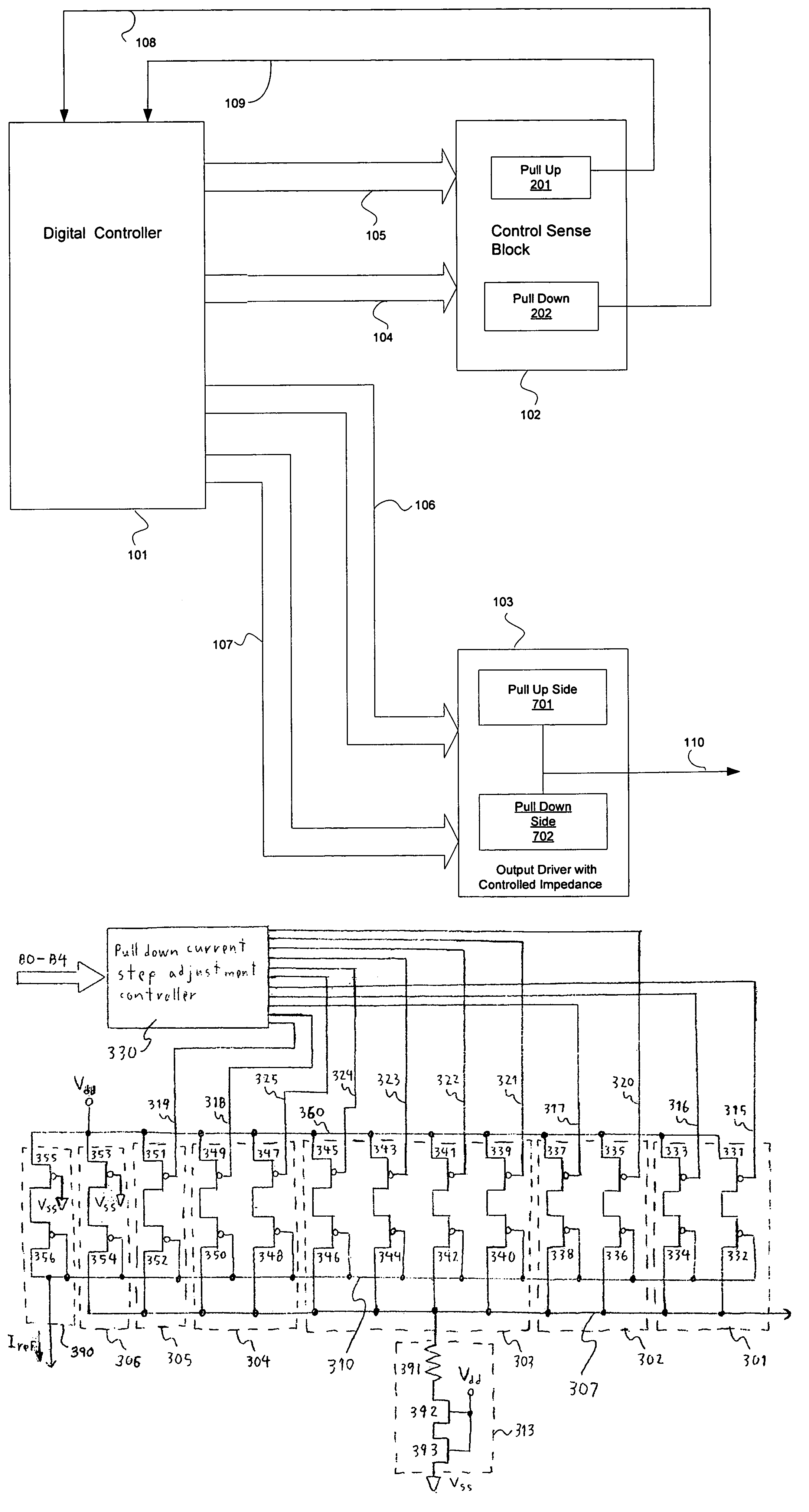
[0191]Referring to FIG. 3, the control block consists of parallel current sources controlled by digital controller. Parallel current sources are scaled versions of external reference current i.e. Vbandgap / Rbias. These currents are dumped in an on-chip replica resistor to maintain reference voltage.

[0192]B0–B4 are control bits that are decoded into following eleven bits using following relationship:

Block 330

Signal 319=B4a=B4

Signal 318=B3a=B3

Signal 325=B3b=B3+B4

Signal 324=B2a=B2

Signal 323=B2b={overscore (B4)}B3B2

Signal 322=B2c=B4B3B2

Signal 321=B2d=B4B3B2

Signal 317=B1a=B1

Signal 320=B1b=B1{overscore ((B3B4))}

Signal 316=B0a=B0

Signal 315=B0b=B0(B1+B2+B3)B4

[0193]Iref=kref×VbandgapRext

(correction needed in FIG. 3)

[0194]Resistance⁢⁢of⁢⁢block⁢⁢313=Rreplica=Rtrim→3+Rdriveα

where a is a factor proportional to physical ratio of Rtrim→3 and Rt. Notice that in this example implementation, Rtrim→3 was used for Resistance#391 and

[0195]Rdrtiv...


PUM


Abstract

An integrated circuit provides dynamic, on chip resistor trimming, including a digital control loop for stabilizing impedance matching among multiple devices communicatively linked over a data transmission line. The digital control loop stabilizes input / output impedance matching of various devices to within a precise ohmic range that is far narrower than standard process variations, such as sheet resistance, within the components themselves. The impedance matching circuit also overcomes EMI problems normally associated with digital control and thus provides dynamic on-chip digital control without non-linearity and with tighter tolerance than is presently possible. Accordingly, the circuit boosts performance of peripheral devices that communicate over a standard USB port, without the need for a computer as a go between or intermediate interface. This makes device to device communication possible as between USB On-the-Go capable devices.

Description

CROSS-REFERENCE TO RELATED APPLICATION[0001]This patent application claims the benefit of U.S. provisional patent application Ser. No. 60 / 536,651, filed Jan. 13, 2004, which is incorporated herein by reference.BACKGROUND[0002]1. Field of the Invention[0003]The field of the present invention relates generally to integrated circuits. In particular, the field of the invention relates to dynamic control for matching of impedance using on-chip components over a high-speed data link or transmission line. A dynamic control circuit enables matching of on-chip impedances with tighter tolerance than the impedance properties inherent in the integrated circuits due to manufacturing process variations.[0004]2. Background of Related Art[0005]There is an increasing need for a system that enables a portable, low power device, such as a cell phone, PDA, or the like to transfer data reliably via a USB (universal serial bus) interface directly to a host device, such as a printer, digital camera, MP3 p...

Claims


Application Information

Patent Timeline
Patent Type & Authority Patents(United States)
IPC IPC(8): H03K17/16
CPCH03K19/0005
Inventor NASRULLAH, JAWAD
Owner TAKLA NABIL
Why Eureka
Try Eureka