Semiconductor device and display device

a semiconductor and display device technology, applied in the field of semiconductor devices and display devices, can solve the problems of reducing the amplitude of the output signal, increasing manufacturing costs and yield, and difficult to make a positive distinction between the source region and the drain region of the tft, so as to prevent the current path from being produced

Inactive Publication Date: 2006-06-27
SEMICON ENERGY LAB CO LTD
View PDF51 Cites 115 Cited by
  • Summary
  • Abstract
  • Description
  • Claims
  • Application Information

AI Technical Summary

Benefits of technology

[0029]As a method of preventing a current path being produced when an input signal is an H level, TFTs 608 an

Problems solved by technology

However, the CMOS circuits require complex manufacturing processes, which leads to an increase in manufacturing cost and to a decrease in yield.
When a logic circuit is composed of unipolar TFTs, for example, N-channel TFTs, there is a problem in that an amplitude of an output signal is reduced as compared with that of an input s

Method used


Image

  • Semiconductor device and display device
  • Semiconductor device and display device
  • Semiconductor device and display device

Examples


embodiment 1

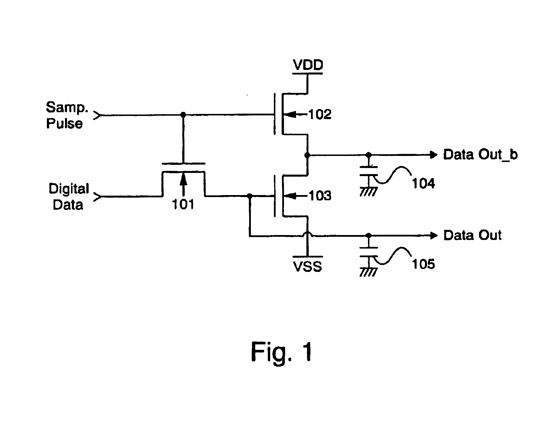
[0150]FIG. 11 shows an example in which the circuit having the configuration described in the embodiment mode is used as a first latch circuit and further a second latch circuit and a buffer are provided. A first latch circuit 111 has TFTs 114 to 116 and capacitor means 117 and 118. A second latch circuit 112 has TFTs 119 and 120 and capacitor means 121 and 122. A buffer circuit 113 has an inverter composed of TFTs 123 to 126 and a capacitor means 127 and an inverter composed of TFTs 128 to 131 and a capacitor means 132.

[0151]When a latch pulse (Latch Pulse) is inputted during a retrace period after sampling corresponding to one horizontal period is completed, the TFTs 119 and 120 in the second latch circuit 112 are turned ON, and signals held in the capacitor means 117 and 118 of the first latch circuit 111 are written into the capacitor means 121 and 122 of the second latch circuit 112.

[0152]When the sampling pulse (Samp. Pulse) becomes an L level to elapse a sampling period, the ...

embodiment 2

[0161]This embodiment gives a description on a method of manufacturing TFTs for driving circuit provided in a pixel portion and in the periphery of the pixel potion formed on the same substrate. A method of manufacturing a liquid crystal display device is described as an example, however, the present invention is not limited to a liquid crystal display device as above mentioned.

[0162]First, as shown in FIG. 7A, a base film 5002 is formed from an insulating film such as a silicon oxide film, a silicon nitride film, and a silicon oxynitride film on a glass substrate 5001. The substrate 5001 is formed of barium borosilicate glass typical example of which is Corning #7059 glass or Corning #1737 glass (product of Corning Incorporated), or of aluminoborosilicate glass. The base film 5002 is, for example, (not shown) a laminate of a silicon oxynitride film that is formed from SiH4, NH3, and N2O by plasma CVD to a thickness of 10 to 200 nm (preferably 50 to 100 nm) and a silicon oxynitride ...

embodiment 3

[0194]In this embodiment, an example in which a display device is actually manufactured using the circuits described in Embodiment Mode and Embodiment 1 will be described.

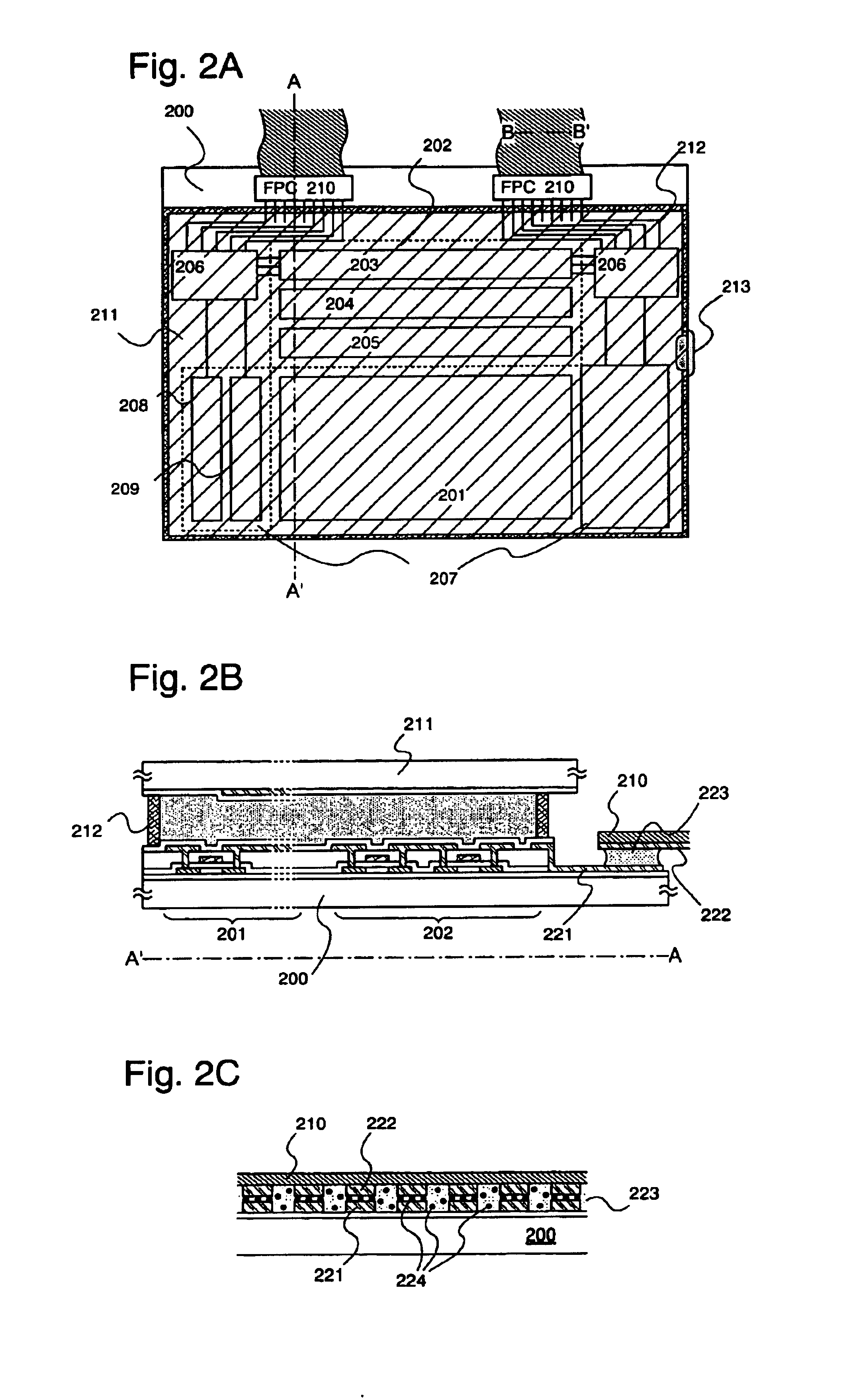
[0195]FIGS. 2A to 2C are schematic views of a display device. A pixel portion 201 is located on a central portion of the substrate 200. A source signal line driver circuit 202 for controlling source signal lines and gate signal line driver circuits 207 for controlling gate signal lines are located in the vicinity of the pixel portion 201. In FIG. 2A, the gate signal line driver circuits 207 are symmetrically located in both sides of the pixel portion 201. It may be located in only one side of the pixel portion 201.

[0196]Signals for operating the source signal line driver circuit 202 and the gate signal line driver circuits 207 which are inputted from an external circuit are inputted through FPCs 210. In this embodiment, the respective signals inputted through the FPCs 210 have small voltage amplitude. Thus, voltage...


PUM


Abstract

A circuit capable of reducing a consumption current is provided for a digital display device composed of unipolar TFTs. There is provided a latch circuit for holding a digital video signal. According to the latch circuit, when the digital video signal is inputted to an input electrode of a TFT (101), a non-inverting output signal is outputted from an output electrode of the TFT (101) and an inverting output signal is outputted from output electrodes of TFTs (102 and 103). Two line outputs of non-inversion and inversion are obtained. Thus, when a buffer located in a subsequent stage is operated, a period for which a direct current path is produced between a high potential and a low potential of a power source can be shortened, thereby contributing to reduction in a consumption current.

Description

BACKGROUND OF THE INVENTION[0001]1. Field of the Invention[0002]The present invention relates to a display device for displaying an image using inputted digital video signals. Note that a display device in this specification includes a liquid crystal display device using a liquid crystal element for a pixel and a light emitting device using a light emitting element represented by an electroluminescence (EL) element. A semiconductor device includes a circuit for performing processing for inputting video signals to pixels arranged in a display device to display an image. Here, more particularly, the semiconductor device includes a pulse output circuit represented by a shift register circuit, a latch circuit, a buffer circuit, a level shift circuit, or the like, or an amplifying circuit represented by an amplifier or the like.[0003]2. Description of the Related Art[0004]Display devices manufactured by forming semiconductor thin films on an insulator such as a glass substrate, in partic...

Claims


Application Information

Patent Timeline
IPC IPC(8): H03K19/0175H03K19/094G02F1/133G09G3/20G09G3/30G09G3/36H03K5/151H03K19/00
CPCG09G3/3688H03K19/0013H03K5/151G09G2310/027G11C27/024
Inventor AZAMI, MUNEHIRO
Owner SEMICON ENERGY LAB CO LTD
Why Eureka
Try Eureka