Organic element for electroluminescent devices

a light-emitting diode and electroluminescent technology, applied in the direction of solid-state devices, discharge tubes/lamp details, natural mineral layered products, etc., can solve the problems of device contamination, device performance limitations, device performance limitations, etc., and achieve low sublimation temperatures and good luminance efficiency

Inactive Publication Date: 2006-08-08
GLOBAL OLED TECH
View PDF11 Cites 4 Cited by
  • Summary
  • Abstract
  • Description
  • Claims
  • Application Information

AI Technical Summary

Benefits of technology

[0019]Such a device exhibits electroluminescence emitting yellow-orange or orange-red light with good luminance efficiency and low sublimation temperatures.

Problems solved by technology

While organic electroluminescent (EL) devices have been known for over two decades, their performance limitations have represented a barrier to many desirable applications.
If the material melts, its use as a dopant is limited.
If the decomposition products also sublime the device can become contaminated.
Decomposition leads to the inefficient use of dopant.
Contamination with decomposition products can cause the device to have shorter operational lifetimes and can contribute to color degradation and light purity.
However, high sublimation temperatures and possible decomposition would limit the use of these rubrene derivatives.
Thus devices containing these rubrene derivatives would fail to provide consistent white OLED devices with high color purity and reduced potential for possible contamination from decomposition impurities in their deposition.

Method used


Image

  • Organic element for electroluminescent devices
  • Organic element for electroluminescent devices
  • Organic element for electroluminescent devices

Examples


example 1

Synthesis (Scheme 1)

[0172]Preparation of compound (3): Under a nitrogen atmosphere, acetylenic compound (2) (5.10 g, 30 mMole), was dissolved in dimethylformamide (DMF) (70 mL) and the solution cool to 0° C. Potassium t-butoxide (KButO) (4.04 g, 36 mMole), was added and the mixture stirred well for approximately 15 minutes. To this mixture was then added the benzophenone (1) (10 g, 30 mMole). Stirring was continued at 0° C. for approximately 30 minutes and then allowed to come to room temperature over a 1-hour period. At the end of this time the solution was cooled to 0° C. and the reaction treated with saturated sodium chloride (20 mL). The mixture was then diluted with ethyl acetate, washed with 2N—HCl (×3), dried over MgSO4, filtered and concentrated under reduced pressure. The crude product was dissolved in 20% ethyl acetate in heptane and subjected to pressure chromatography over silica gel eluting with the same solvent mixture. The main material was collected. Yield of compoun...

example 2

Sublimation Temperatures

[0174]The sublimation temperatures at 5×10⁻⁶ Torr needed to deposit the inventive and comparative dopants at 1% and 2%-wt. of the host are recorded in Table 1. This sublimation temperature is the temperature required to sublime a specific amount of material, recorded as thickness, onto the device at a specific rate and is given in Angstroms / sec., (A / s). For dopants at 1%-wt of host, this rate is 0.04 A / s and at 2%-wt it is 0.08 A / s. The samples shown in the table are divided into groups, each group with its own comparative dopant. Comp-1 is the comparative example for Inv-1 through Inv-4; Comp-2 is the comparative example for Inv-5, Inv-6 and Inv-9; Comp-3 is the comparative example for Inv-15; and Comp-4 is the comparative example for Inv-23 and Inv-24. The comparative dopants have the same basic structure as the inventive dopants in its group but without the fluorine or fluorine-containing group. Comp-1 is the parent rubrene. It is well known to those in th...

example 3

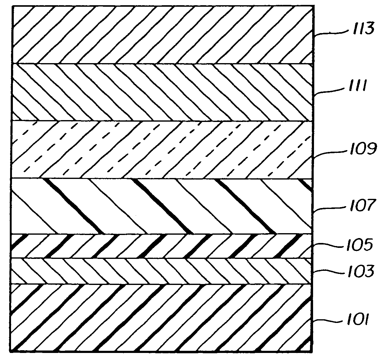
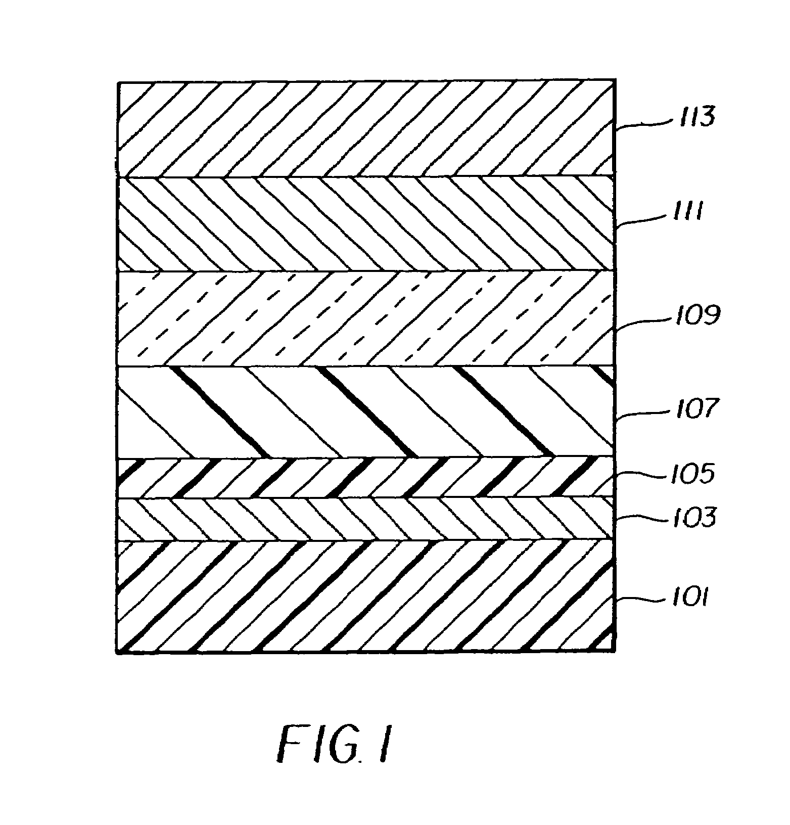
EL Device Fabrication—Inventive Example

[0178]An EL device satisfying the requirements of the invention was constructed as Sample 15 in the following manner:

[0179]A glass substrate coated with an 85 nm layer of indium-tin oxide (ITO) as the anode was sequentially ultrasonicated in a commercial detergent, rinsed in deionized water, degreased in toluene vapor and exposed to oxygen plasma for about 1 min.

[0180]a) Over the ITO was deposited a 1 nm fluorocarbon (CFx) hole-injecting layer (HIL) by plasma-assisted deposition of CHF3.

[0181]b) A hole-transporting layer (HTL)of N,N′-di-1-naphthalenyl-N,N′-diphenyl-4,4′-diaminobiphenyl (NPB) having a thickness of 150 nm was then evaporated from a tantalum boat.

[0182]c) A 37.5 nm light-emitting layer (LEL) of tris(8-quinolinolato)aluminum (III) (AlQ3) and Inv-1 (2%-wt, see Table 2) were then deposited onto the hole-transporting layer. These materials were also evaporated from tantalum boats.

[0183]d) A 37.5 nm electron-transporting layer (ETL) of...


PUM

PropertyMeasurementUnit
wavelengthaaaaaaaaaa
wavelength of maximum emissionaaaaaaaaaa
sublimation temperatureaaaaaaaaaa

Abstract

Disclosed is an OLED device comprising a light-emitting layer (LEL) containing a host and an emitting dopant located between a cathode and an anode wherein the dopant is a naphthacene derivative represented by formula (I):wherein:a) said naphthacene derivative contains at least one fluorine or fluorine containing group; andb) when exactly two fluorine containing groups are present said groups are not located at the 5- and 12-positions or at the 6- and 11-positions.

Description

FIELD OF INVENTION[0001]This invention relates to organic light emitting diode (OLED) electroluminescent (EL) device comprising a light-emitting layer containing a naphthacene dopant compound containing fluorine or fluorine-containing groups.BACKGROUND OF THE INVENTION[0002]While organic electroluminescent (EL) devices have been known for over two decades, their performance limitations have represented a barrier to many desirable applications. In simplest form, an organic EL device is comprised of an anode for hole injection, a cathode for electron injection, and an organic medium sandwiched between these electrodes to support charge recombination that yields emission of light. These devices are also commonly referred to as organic light-emitting diodes, or OLEDs. Representative of earlier organic EL devices are Gurnee et al. U.S. Pat. No. 3,172,862, issued Mar. 9, 1965; Gurnee U.S. Pat. No. 3,173,050, issued Mar. 9, 1965; Dresner, “Double Injection Electroluminescence in Anthracene...

Claims


Application Information

Patent Timeline
Patent Type & Authority Patents(United States)
IPC IPC(8): H05B33/14H01L27/32H01L51/50H01L51/52H01L51/54C07C15/38H01L51/00H01L51/30
CPCC07C15/38H01L51/0054H01L51/0059H01L51/0062Y10S428/917H01L51/0085H01L51/0089H01L51/5012H01L51/5036H01L51/0084H10K85/622H10K85/649H10K85/631H10K85/341H10K85/351H10K85/342H10K50/125H10K50/11
Inventor BEGLEY, WILLIAM J.HATWAR, TUKARAM K.RAJESWARAN, MANJUANDRIEVSKY, NATASHA
Owner GLOBAL OLED TECH
Why Eureka
Try Eureka