Semiconductor device and method of manufacturing the same

a technology of semiconductor devices and semiconductors, applied in semiconductor devices, semiconductor/solid-state device details, electrical apparatus, etc., can solve the problem of excessive etching of dcs-sin films, and achieve the effect of reducing leakage curren

Inactive Publication Date: 2006-08-29
TOSHIBA MEMORY CORP
View PDF8 Cites 7 Cited by
  • Summary
  • Abstract
  • Description
  • Claims
  • Application Information

AI Technical Summary

Benefits of technology

[0026]However, a ratio in the polishing rate by CMP of the interlayer insulating film (SiO2) to the silicon nitride film (DCS-SiN film) formed by this method is about 30. As a result, the DCS-SiN film is excessively etched in the step of removing by CMP the excess DCS-SiN film outside the wiring trench so as to increase the leakage current between the buried wiring and the lower capacitor electrode.
[0062]Still further, the silicon oxide film containing chlorine is also allowed to contain at least one of phosphorus and boron so as to obtain additional effects that the gettering of impurities and selectivity ratio in the etching step are improved.

Problems solved by technology

As a result, the DCS-SiN film is excessively etched in the step of removing by CMP the excess DCS-SiN film outside the wiring trench so as to increase the leakage current between the buried wiring and the lower capacitor electrode.

Method used


Image

  • Semiconductor device and method of manufacturing the same
  • Semiconductor device and method of manufacturing the same
  • Semiconductor device and method of manufacturing the same

Examples


first embodiment

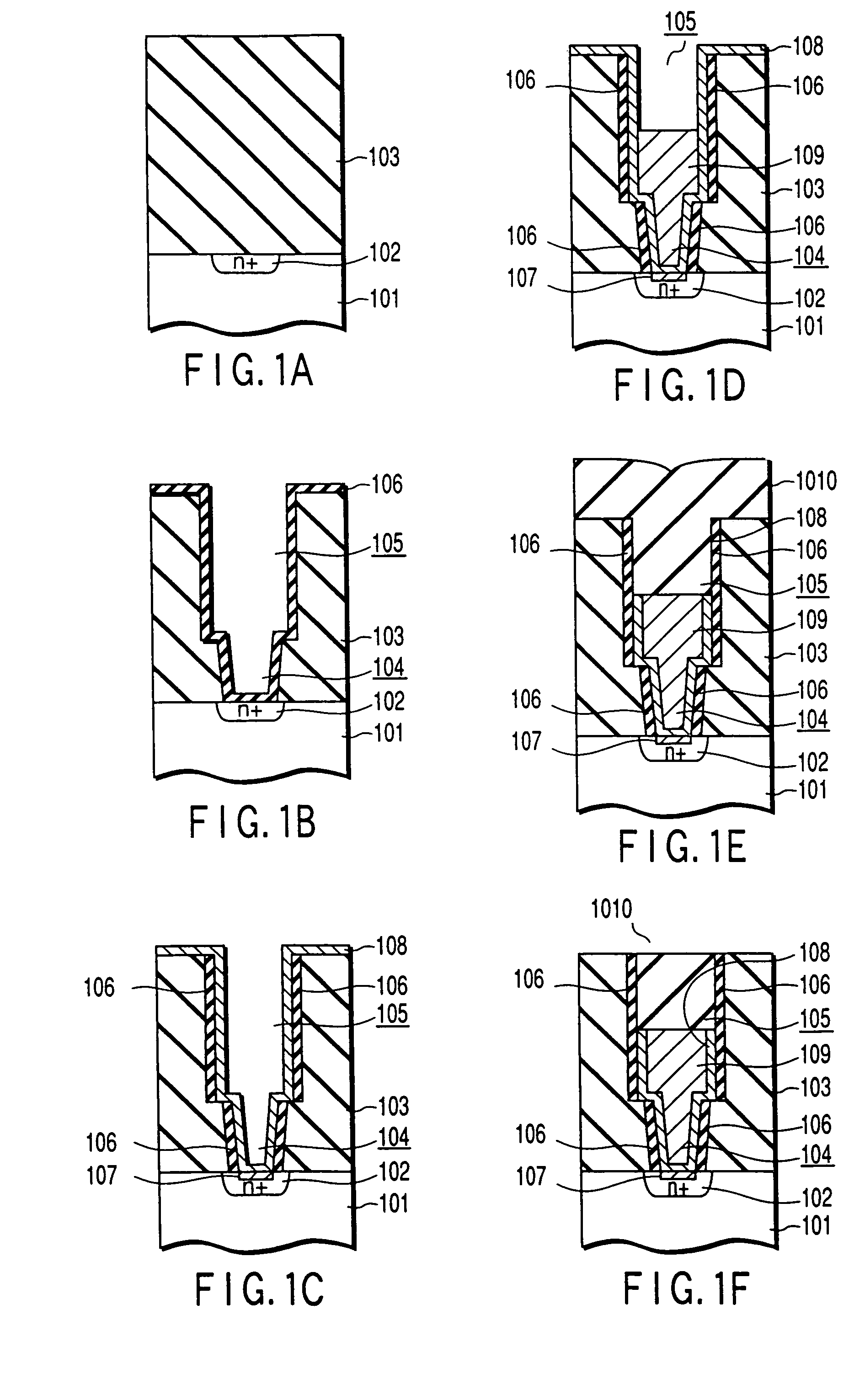
[0105]FIGS. 1A to 1F are cross sectional views collectively showing a method of manufacturing a semiconductor device according to a first embodiment of the present invention. These drawings show cross sections in a direction perpendicular to the longitudinal direction of the channel of a MOS transistor of a DRAM cell.

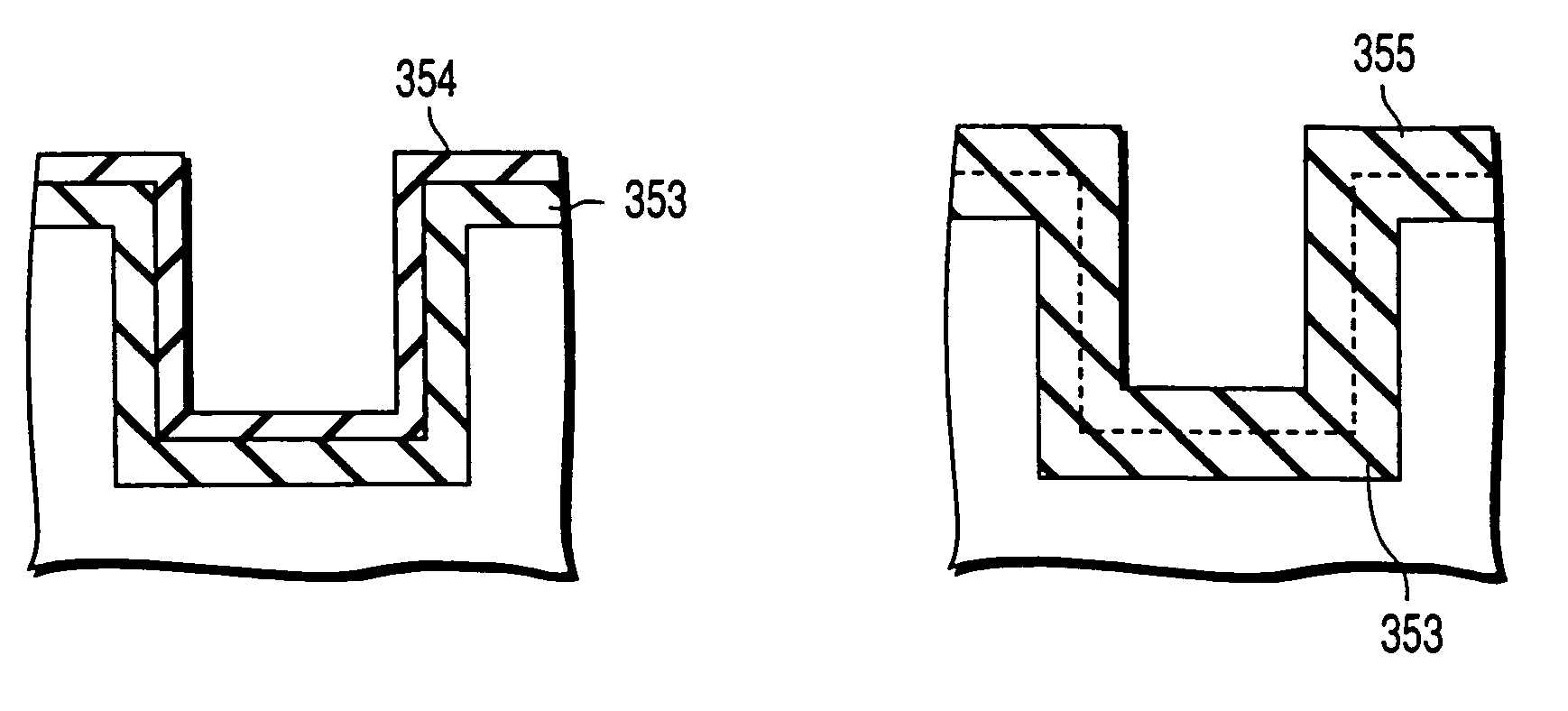
[0106]In the first step, an n-type drain diffusion layer 102, etc. are formed by a known method in a silicon substrate 101 to finish forming a MOS transistor, followed by forming an interlayer insulating film (SiO2 film) 103 on the entire surface, as shown in FIG. 1A. Then, a contact hole 104 exposing the n-type drain diffusion layer 102 and a wiring trench 105 connected to the n-type drain diffusion layer 102 via the contact hole 104 are formed in the interlayer insulating film 103, followed by forming a silicon nitride film 106 over the entire surface, as shown in FIG. 1B. The silicon nitride film 106 thus formed is selectively removed by RIE (reactive ion etching) su...

second embodiment

[0133]The first embodiment is directed to formation of a silicon nitride film having a high chlorine concentration. On the other hand, the second embodiment is directed to formation of a silicon nitride film having a high chlorine concentration and containing an excess silicon. FIGS. 1A to 1F will also be used for describing the second embodiment.

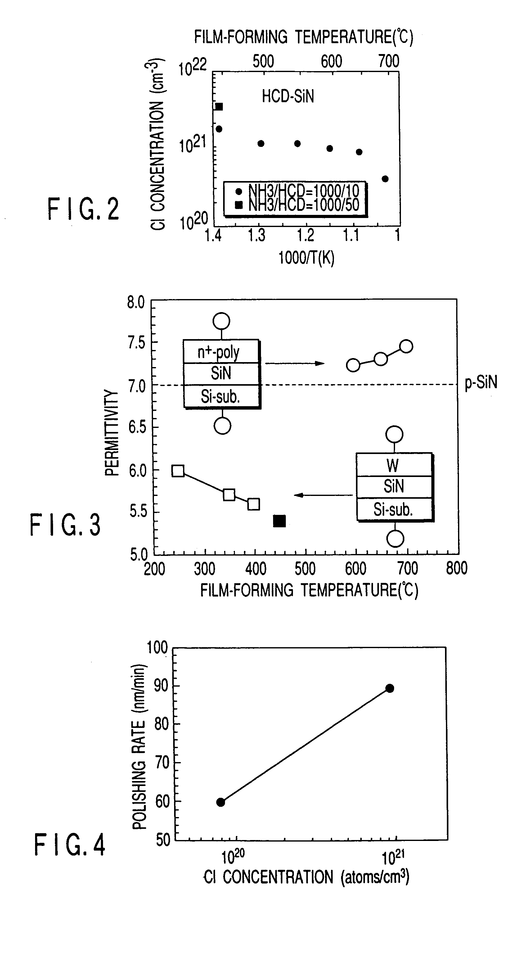
[0134]The second embodiment is equal to the first embodiment up to the step shown in FIG. 1D. Then, a silicon nitride film (HCD-SiN film) 10 is formed on the entire surface in a manner to fill the inner space of the wiring trench 6 by an LPCVD method using a mixed gas consisting of Si2Cl6 and NH3, as shown in FIG. 1E. The silicon nitride film 10 is formed at a temperature of 600° C., a reactor inner pressure of 0.5 Torr, and a NH3 / Si2Cl6 flow rate ratio of 2000 sccm / 20 sccm. The film-forming rate is 1.4 nm / min.

[0135]In the next step, the excess HCD-SiN film 10 outside the wiring trench 6 is removed by CMP under the conditions equal to those...

third embodiment

[0146]With progress in miniaturization of the device element, it is necessary to decrease the resistance of the gate electrode. Therefore, it is necessary in the next era to change the polymetal gate structure employed nowadays into a metal gate electrode. On the other hand, since it is difficult to achieve fine processing of a metal film by etching, a damascene gate process (A. Yagishita, et al., IEDM Tech. Digest, 1998: p. 785) is employed for forming a metal gate electrode. Also, a dummy gate is required for forming a trench in which the metal gate electrode is buried. A method of manufacturing a MOS transistor by using a metal gate electrode according to a third embodiment of the present invention will now be described with reference to FIGS. 11A to 11I.

[0147]In the first step, a shallow trench is formed in a surface region of a silicon substrate 121, followed by forming a thermal oxide film 122 on the entire surface and subsequently burying a device element separating insulatin...


PUM


Abstract

Hexachlorodisilane (Si2Cl6) is used as a Si raw material for forming a silicon nitride film that can be widely different in the etching rate from a silicon oxide film. The silicon nitride film is formed by an LPCVD method.

Description

[0001]This is a division of application Ser. No. 09 / 984,404, filed Oct. 30, 2001 now U.S. Pat. No. 6,790,723, which is a divisional of application Ser. No. 09 / 478,369, filed Jan. 6, 2000 (now U.S. Pat. No. 6,333,547), both of which are incorporated in their entirety herein by reference.BACKGROUND OF THE INVENTION[0002]The present invention relates to a semiconductor device including a silicon nitride film containing chlorine and a method of manufacturing the same.[0003]With progress in the degree of integration and fineness of the semiconductor device, a semiconductor device of the next era makes it absolutely necessary to develop a process technology that permits forming an interlayer insulating film (SiO2 film) having a finer contact hole of a higher aspect ratio, that permits forming a uniform silicon nitride film of a high step coverage within the contact hole made in the interlayer insulating layer, and that permits polishing the silicon nitride film by a chemical mechanical po...

Claims


Application Information

Patent Timeline
Patent Type & Authority Patents(United States)
IPC IPC(8): H01L21/76H01L21/318H01L21/336H01L21/60H01L21/768H01L21/8242H01L23/485H01L23/522H01L27/108H01L29/78
CPCH01L21/3185H01L21/76801H01L21/76802H01L21/76807H01L21/76826H01L21/76831H01L21/76834H01L21/76879H01L21/76897H01L23/485H01L2924/0002H01L27/10873H01L2924/00H01L21/76883H01L21/02271H01L21/02126H01L21/02208H01L21/02211H01L21/02129H01L21/02167H01L21/0217H10B12/05
Inventor TANAKA, MASAYUKISAIDA, SHIGEHIKOTSUNASHIMA, YOSHITAKA
Owner TOSHIBA MEMORY CORP
Why Eureka
Try Eureka