Semiconductor material, field effect transistor and manufacturing method thereof

a technology of field effect transistor and semiconductor material, which is applied in the direction of semiconductor devices, electrical devices, nanotechnology, etc., can solve the problems of large number of problems to be solved, metal pollution, heavy metal pollution, etc., and achieve the reduction of accurate formation, and the effect of reducing the collection rate of silicon wires

Inactive Publication Date: 2006-09-19
HITACHI LTD
View PDF5 Cites 22 Cited by
  • Summary
  • Abstract
  • Description
  • Claims
  • Application Information

AI Technical Summary

Benefits of technology

[0018]In the above-described process using the lift-off by hydrofluoric acid after processing the SOI substrate by the lithography, the problems of the metal contamination and the variation of the wire shape can be solved. This is because the metal pollution does not occur when the SOI substrate is processed in a clean room and the wire shape can be accurately formed within the range of the process accuracy when it is processed by the usual silicon process using the lithography. Therefore, under the present situation, the silicon wire with a diameter of several μm to sub μm formed by the top-down process is more preferable than the silicon nanowire formed by the bottom-up process from the view point of the integration.
[0019]However, when using the lift-off by hydrofluoric acid, it is difficult directly collect the silicon wires dispersed in the hydrofluoric acid solution. The silicon wires can be collected by means of substitution for solutions such as water. However, the collection rate of the silicon wires is reduced due to the process of the substitution. Furthermore, since it is necessary to make a dilution many times so as to remove the hydrofluoric acid in the process of the substitution, the collection rate of the silicon wires is extremely reduced. Also, the method using the filtration may be available. However, the new filter for filtering the silicon nanowires from the hydrofluoric acid is required. Further, when the silicon wires are arranged on a substrate such as a glass substrate which is dissolved by hydrofluoric acid and the hydrofluoric acid is not completely removed by the substitution, the glass substrate may be damaged by the hydrofluoric acid.
[0021]Also, the above-described manufacturing method of the silicon wires using the SOI substrate has the problem of high cost. The SOI substrate is far more expensive than the normal silicon substrate. As described above, in order to achieve the application to the flexible transistor, it is indispensable to fabricate the device by a low-cost process such as the printing process. In consideration of the problems described above, the first object of the present invention is to provide a manufacturing method of a silicon wire in which the lithography capable of reducing the metal pollution and processing the wires into a desired shape is used and the silicon wires are not dispersed into hydrofluoric acid, a silicon wire transistor using the silicon wire, and a manufacturing method of the silicon wire transistor.
[0022]The second object of the present invention is to provide a manufacturing method of a silicon wire in which a thermal oxidation film is formed around silicon wires at high temperature and the silicon wires are collected without removing the thermal oxidation film by hydrofluoric acid, a silicon wire transistor using the silicon wires covered with the thermal oxidation film, and a manufacturing method of the silicon wire transistor. Also, the third object of the present invention is to provide a method for manufacturing the silicon wires by a low-cost process in comparison to the case using an SOI substrate, a silicon wire transistor using the silicon wires, and a manufacturing method of the silicon wire transistor.
[0024]As the representative effects of the present invention, a high-quality semiconductor material can be provided, and a good flexible device can be provided.

Problems solved by technology

However, there are a lot of problems to be solved for the practical use of the silicon wire transistor.
The problem in the formation of the silicon nanowire by the bottom-up process using the metal nanoparticles is the metal pollution.
However, the heavy metal pollution occurs since the silicon nanowires are formed around the metal nanoparticles.
Particularly, since heavy metal such as gold rapidly disperses into silicon, the mass production of the silicon wire transistor is difficult when the silicon nanowires polluted by the heavy metal are used in the fabrication process.
Therefore, the width and the length of the silicon nanowires are not uniform.

Method used


Image

  • Semiconductor material, field effect transistor and manufacturing method thereof
  • Semiconductor material, field effect transistor and manufacturing method thereof
  • Semiconductor material, field effect transistor and manufacturing method thereof

Examples


first embodiment

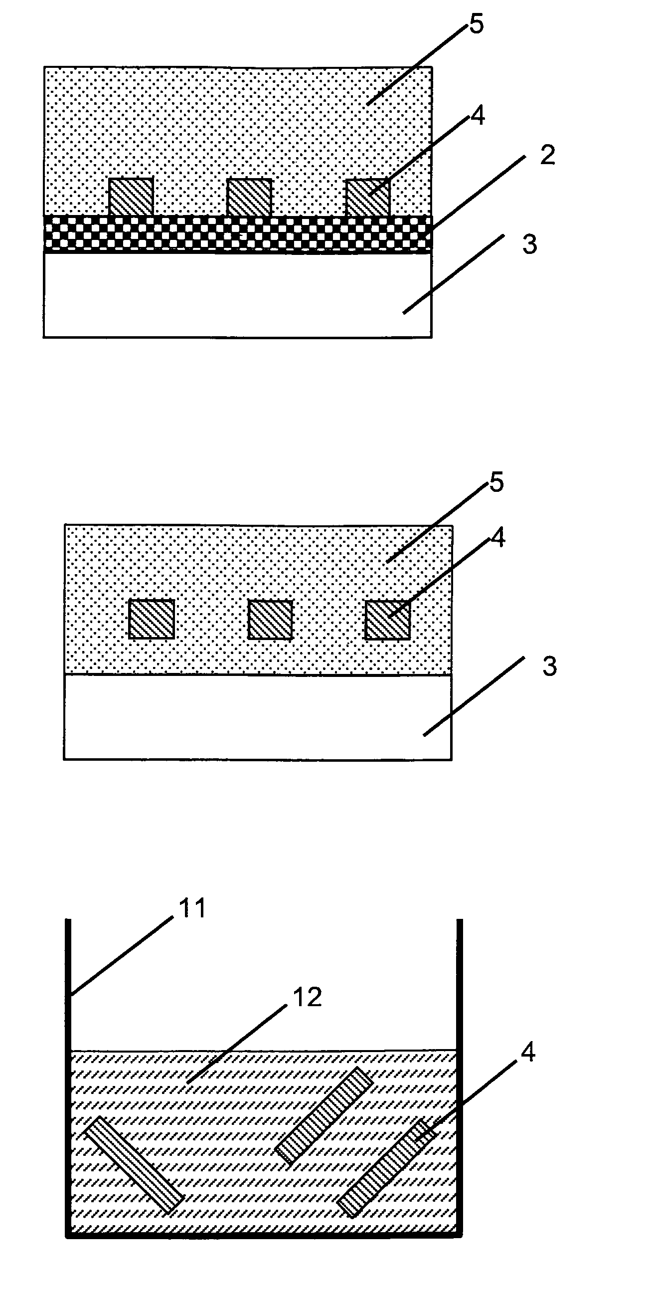
[0092]In this embodiment, a method of manufacturing a semiconductor material in which a bridge structure is formed so as to collect the silicon wires without using the lift-off of the silicon wires in the hydrofluoric acid solution and a method of forming a flexible transistor using the silicon wires will be disclosed.

[0093]First, an SOI (Silicon-On-Insulator) substrate comprised of a silicon layer 1, an oxide film 2, and a silicon substrate 3 as shown in FIG. 2 is prepared. In the SOI substrate, the silicon layer 1 is made of single crystal silicon. The size of the SOI substrate is 8 inches, the thickness of the silicon layer 1 is 200 nm, the thickness of the oxide film 2 serving as a BOX layer is 200 nm, and the thickness of the silicon substrate 3 is 500 μm. In order to reduce the contact resistance with electrodes, the doping is performed to the silicon layer. Boron is implanted into the silicon wire operated as a p type storage transistor until its concentration reaches 1×10¹⁷ ...

second embodiment

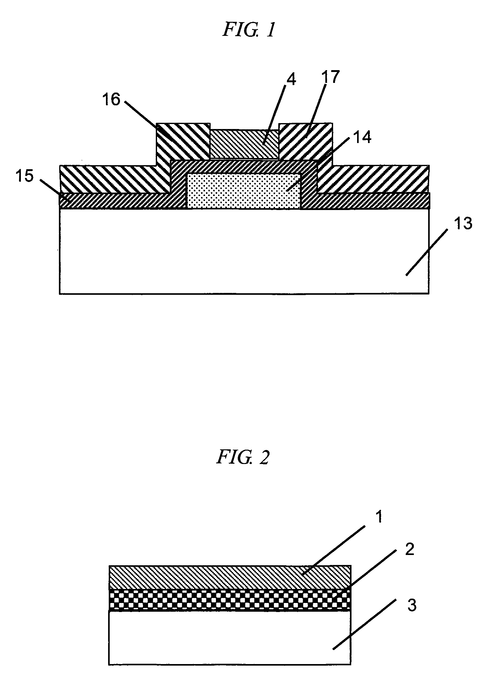
[0108]For the achievement of the second object of the present invention, a method of forming a silicon wire transistor will be described, in which after forming the silicon bridge, a thermal oxide film is formed around the silicon wires at a high temperature, and the thermal oxide film is used as the gate insulating film. First, the bridge structure of the silicon wires 4 as shown in FIG. 8 is formed in the same manner as that of the first embodiment. In this second embodiment, the silicon layer 1 is doped to both p type and n type. The silicon wire 4 doped to p type is operated on the inversion side and thus functions as an nMOS, and the silicon wire 4 doped to n type is operated on the storage side and thus functions as a pMOS. In this manner, the nMOS is fabricated in a desired region on a substrate and the pMOS is fabricated in a different region on the same substrate. By doing so, the CMOS (Complementary MOS) circuit can be incorporated.

[0109]FIG. 56 is an enlarged cross-sectio...

third embodiment

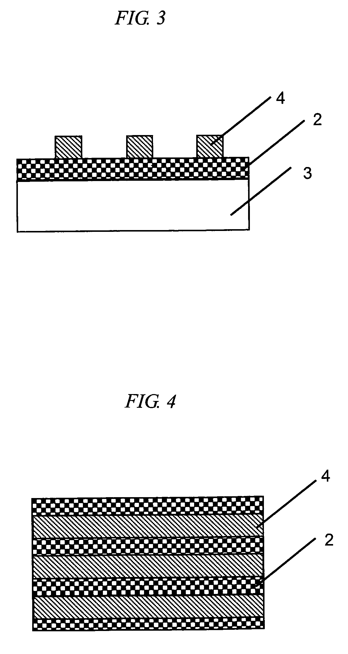
[0128]The second embodiment discloses the method of collecting the silicon wires 4, around which the gate insulating film 19 fabricated by the high-temperature oxidation process is formed, without losing the gate insulating film 19. However, the processing techniques used in the standard silicon process, for example, the lithography process, the ion implantation, and the high-temperature activation process are required in order to fabricate the transistor in accordance with the method described in the second embodiment. Therefore, the application to the flexible transistor is difficult due to the high cost. This third embodiment discloses the technology in which the high-cost processing technique, for example, the lithography process is not used after collecting the silicon wires 4, and the silicon wire transistor is fabricated on the plastic substrate by using the printing method in a self-aligned manner.

[0129]First, the silicon wires 4 around which the gate insulating film 19 is f...


PUM

PropertyMeasurementUnit
frequencyaaaaaaaaaa
thicknessaaaaaaaaaa
thicknessaaaaaaaaaa

Abstract

The silicon wires formed around metal particles by crystal growth have the problem of metal pollution. For its solution, in the present invention, a silicon bridge is formed through standard silicon processes such as the lithography and the wet etching using hydrofluoric acid performed to an SOI substrate. Thereafter, a thermal oxide film is desirably formed at a high temperature to form a high-quality gate insulating film. It is also desirable to form a coaxial gate electrode. Then, after burying the bridge sections of the silicon bridge in a resist film, the silicon on the bridge girders is removed, and thereafter, the silicon wires buried in the resist film are collected. In this manner, the silicon wires can be collected without dispersing into the hydrofluoric acid solution. Then, a transistor using the silicon wires as a channel is formed.

Description

CROSS-REFERENCE TO RELATED APPLICATION[0001]The present application claims priority from Japanese Patent Application JP 2004-311719 filed on Oct. 27, 2004, the content of which is hereby incorporated by reference into this application.TECHNICAL FIELD OF THE INVENTION[0002]The present invention relates to a field effect transistor and a manufacturing method thereof. More particularly, it relates to a field effect transistor which can be fabricated on an intended substrate such as a flexible plastic substrate because a wire-shaped semiconductor is used for the channel material and a manufacturing method thereof, and it also relates to the wire-shaped semiconductor and a manufacturing method thereof.BACKGROUND OF THE INVENTION[0003]In the modern information society, the semiconductor is used in all sorts of things. For example, not to speak of the personal computer and the mobile phone, the semiconductor is used in all of digital consumer electronics such as the flat panel display, the...

Claims


Application Information

Patent Timeline
Patent Type & Authority Patents(United States)
IPC IPC(8): H01L21/00H01L21/84
CPCB82Y10/00H01L27/12H01L29/0673H01L29/42392H01L29/66772H01L27/1292H01L29/78696Y10S977/762Y10S977/932Y10S977/723Y10S977/937H01L29/78603
Inventor SAITO, SHINICHIARAI, TADASHIPARK, SEONG-KEEMINE, TOSHIYUKI
Owner HITACHI LTD
Why Eureka
Try Eureka