Method for fabrication of polycrystalline silicon thin film transistors

a technology of polycrystalline silicon and thin film, which is applied in the direction of basic electric elements, semiconductor devices, electrical equipment, etc., can solve the problems of reducing the uniformity, limiting the size of silicon grains, and affecting the electrical properties of components, so as to reduce the differences between components, enhance the resolution of display, and facilitate the effect of mobility

Inactive Publication Date: 2006-10-03
NAT CHIAO TUNG UNIV
View PDF11 Cites 10 Cited by
  • Summary
  • Abstract
  • Description
  • Claims
  • Application Information

AI Technical Summary

Benefits of technology

[0006]The main purpose of the present invention is to provide a high mobility for the field effect carrier of the LTPS-TFT and to diminish the differences among components. On fabricating the transistors according to the present invention, if the channel width is smaller but the silicon grain in the channel is larger, the transistors that produce driving pixels can conspicuously enhance the resolution of the display. Moreover, the process window for laser recrystallization becomes wider and the electrical properties of the LTPS-TFT are enhanced. In the mean time, the differences among components are diminished, the uniformity among them is improved and the product yield is increased.
[0007]The other purpose of this invention is to obtain a mechanism that the melting of the silicon and the lateral recrystallization is triggered after the annealing of a continuous-wave (CW) laser or an excimer laser. Such a mechanism can greatly improve the mobility of the field effect carrier to enhance the characteristics of the components without additional mask during the production. In addition, the thick silicon spacer can guarantee the active layer against shrinkage after laser irradiation. If the active layer in dog-bone shape is scanned by a high-energy CW laser in a source-drain direction, a single silicon grain can be obtained in the channel of the transistor which can be further used to produce LTPS-TFT with high performance and good uniformity. On obtaining components with bigger channel width W according to the present invention, various current requirements can be met by parallel connections of several channels with smaller width Wi so that bigger silicon grain can still be kept in the channel and the self-heating effect can be solved at the same time.

Problems solved by technology

However, on producing the LTPS-TFT by laser annealing, the active layer of the transistor is formed after the laser recrystallization of the a-Si film, so that the resulting silicon grain structure would be limited in size owing to the thickness of the film.
And the silicon grains with irregular sizes are spread in the active layer of the transistor, which causes the differences in the electric properties of the components and so diminishes the uniformity.
But, on the contrary, if the active layer of transistor is formed ‘before’ the laser recrystallization of the a-Si film, a surface tension induced shrinkage would happen on the active layer owing to the melting of the whole silicon film.
Therefore, the conventional method can not be used in fabricating LTPS-TFTs.
In addition, the structure of the components, like TFT and silicon-on-insulator metal oxide semiconductor field effect transistor (SOI-MOSFET), would comprise an insulated layer with poor thermo conductivity under active layer.

Method used


Image

  • Method for fabrication of polycrystalline silicon thin film transistors
  • Method for fabrication of polycrystalline silicon thin film transistors
  • Method for fabrication of polycrystalline silicon thin film transistors

Examples


Embodiment Construction

[0021]The following descriptions of the preferred embodiment are provided to understand the features and the structures of the present invention.

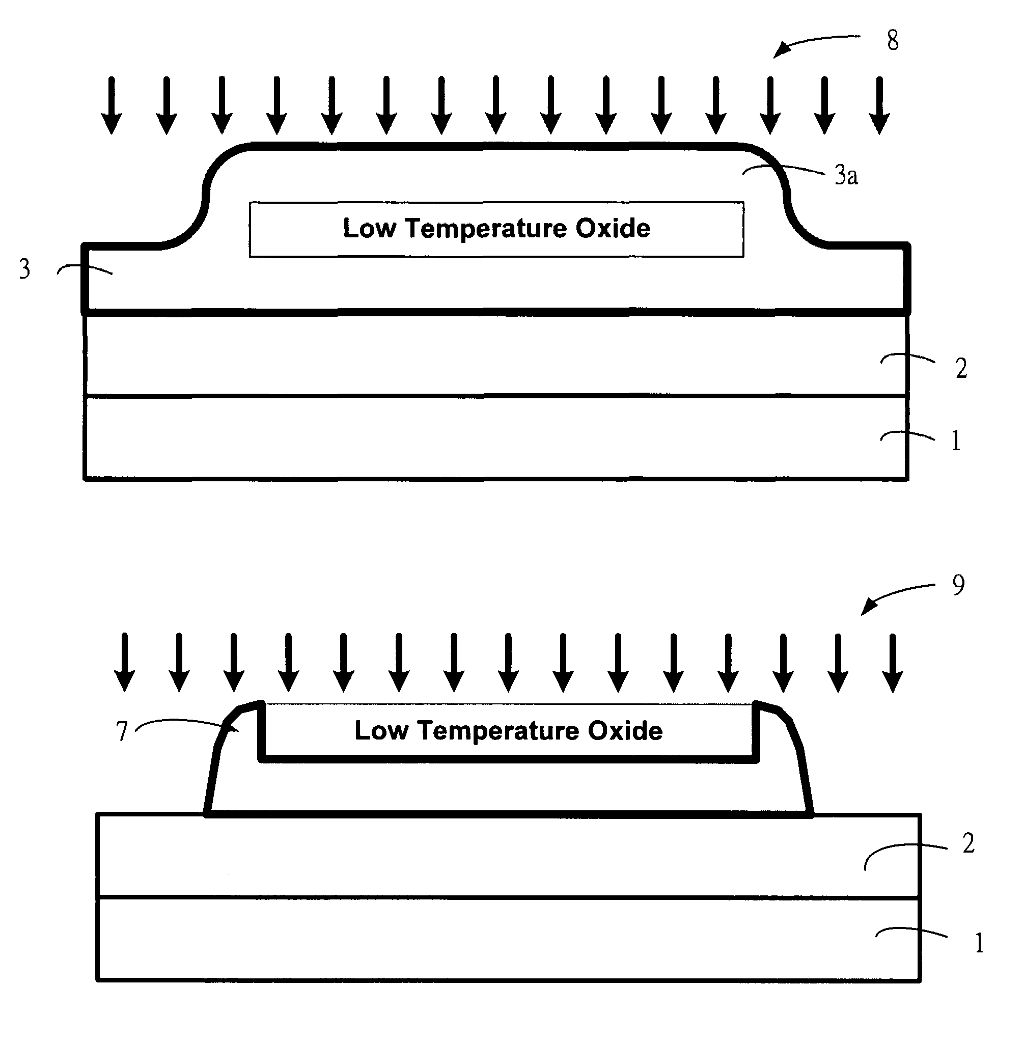
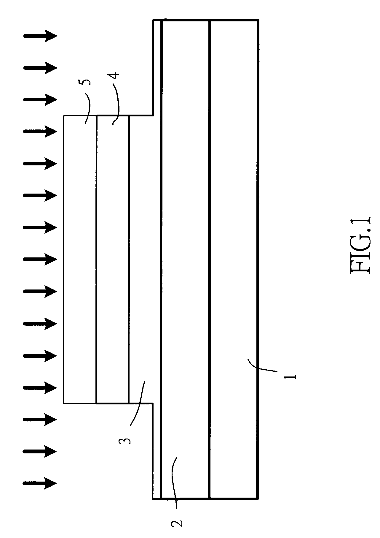
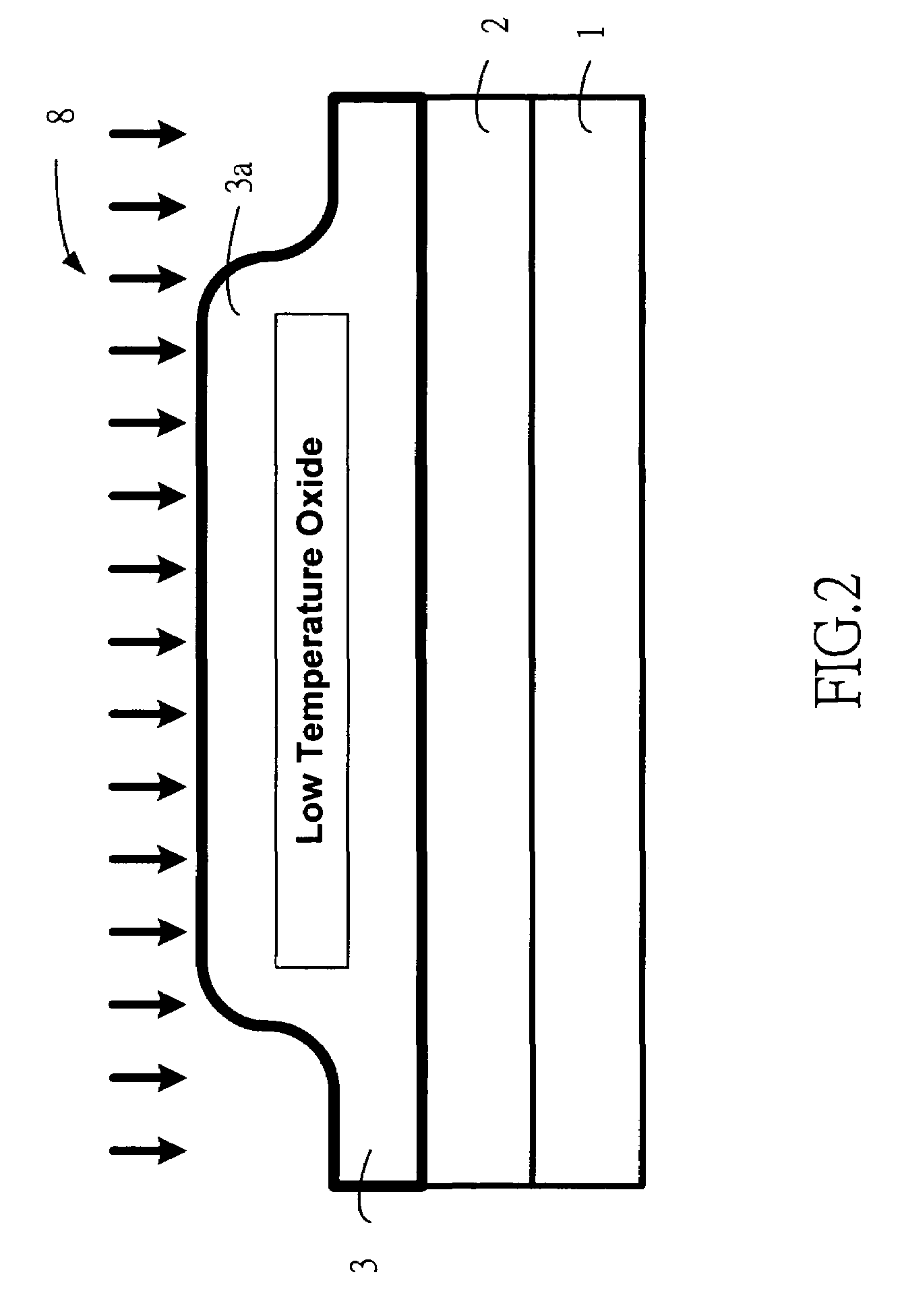
[0022]Please refer to FIG. 1 to FIG. 7, which are cross-sectional views showing the forming process in vertical current direction according to the present invention; a vertical view showing the relative positions of the drain, the source, and the gate in the transistor according to the present invention; a SEM (scanning electron microscope) view according to the present invention; a view showing the positions of the graphs on the active layer and the scan direction of the recrystallization done by a continuous-wave (CW) laser according to the present invention; and a view showing the way to overcome the self-heating effect of the transistor with bigger channel width according to the prior art. As shown in the figures, the present invention is a method for fabrication of polycrystalline silicon thin film transistors, comprising the following...


PUM

PropertyMeasurementUnit
temperatureaaaaaaaaaa
anisotropicaaaaaaaaaa
dielectricaaaaaaaaaa

Abstract

The present invention provides a method for fabrication of polycrystalline silicon thin film transistors, which forms a silicon spacer on the sidewall of the active layer of a thin film transistor (TFT) by way of anisotropic plasma etching in a single direction. The silicon spacer provides a mechanism for laser recrystallization on the sidewall to prevent the active layer from shrinkage or shelling-off after the laser recrystallization. According to the present invention, large grains can be formed in the channel without additional mask during production. By doing so, the characteristics of the components are enhanced; the uniformity is improved; and, the production cost is lowered. Therefore, this technique will play an important role in the fields of low temperature polycrystalline silicon thin film transistor (LTPS-TFT).

Description

RELATED APPLICATION[0001]This application is a Continuation-In-Part of application Ser. No. 10 / 601,701, filed on Jun. 24, 2003 and currently pending.FIELD OF THE INVENTION[0002]The present invention relates to a method for fabrication of polycrystalline silicon thin film transistors. More particularly, the present invention relates to obtaining large silicon grains in the channel of the transistor without any additional mask so to enhance the characteristics, to improve the uniformity, and to lower the production cost.BACKGROUND OF THE INVENTION[0003]As the price of the conventional a-Si (amorphous silicon) TFT (thin film transistor) LCD (liquid crystal display) keeps going down and the applications of the LTPS-TFT (low temperature polycrystalline silicon thin film transistor) in small-size display is extending day by day, the LTPS-TFT has gained its market share in mobile terminal devices, such as personal digital assistant, digital camera, cell phone, etc., because of its advantag...

Claims


Application Information

Patent Timeline
Patent Type & Authority Patents(United States)
IPC IPC(8): H01L21/00H01L21/20H01L21/336H01L21/77
CPCH01L21/2026H01L27/1281H01L29/66757H01L27/1296H01L21/02686H01L21/02683H01L21/02488H01L21/02532H01L21/02691H01L21/02595
Inventor YEH, CHING-FACHEN, TIEN-FULOU, JEN-CHUNG
Owner NAT CHIAO TUNG UNIV
Why Eureka
Try Eureka