Polymeric antireflective coatings deposited by plasma enhanced chemical vapor deposition

a technology of chemical vapor deposition and anti-reflective coatings, which is applied in the direction of resistive material coatings, plasma techniques, metallic material coating processes, etc., can solve the problems of insufficient planarization, limited performance, and magnified inherent inefficiencies of the spin coating process, so as to minimize negative effects, reduce overall waste, and minimize was

Inactive Publication Date: 2006-11-07
BREWER SCI
View PDF40 Cites 5 Cited by
  • Summary
  • Abstract
  • Description
  • Claims
  • Application Information

AI Technical Summary

Benefits of technology

[0044]Finally, in addition to the aforementioned antireflective layer properties, the instant invention has a further distinct advantage over prior art spincoating methods which utilize large quantities of solvents. That is, the instant methods avoid spincoating solvents which...

Problems solved by technology

While spincoated antireflective layers offer excellent reflectivity control, their performance is limited by their nonuniformity, defectivity and conformality constrictions, and other inefficiencies inherent within the spincoating process.
As the industry approaches the adoption of eight-inch or even twelve-inch semiconductor substrates, the inherent inefficiencies of the spincoating process become magnified.
Although high optical density at DUV wavelengths enable these pre-designed polymers to provide effective reflectivity control at prior art dimensions, they have numerous drawbacks.
Another problem with the currently available antireflective coating application processes is inadequate planarization.
The formed layers typically lack uniformity in that the thickness at the edge of the substrate is greater than the thickness at the center.
Furthermore, spincoated antireflective coating layers tend to planarize or unevenly coat surface topography rather than form highly conformal layer...

Method used


Image

  • Polymeric antireflective coatings deposited by plasma enhanced chemical vapor deposition
  • Polymeric antireflective coatings deposited by plasma enhanced chemical vapor deposition
  • Polymeric antireflective coatings deposited by plasma enhanced chemical vapor deposition

Examples


examples

[0064]The following examples set forth preferred methods in accordance with the invention. It is to be understood, however, that these examples are provided by way of illustration and nothing therein should be taken as a limitation upon the overall scope of the invention.

Materials and Methods

examples 1-3

[0065]The PECVD process to which the antireflective compounds were subjected in the following Examples 1-3 involved subjecting the compounds to sufficient electric current and pressure so as to cause the solid or liquid compounds to form a plasma. The monomers to be deposited were initially weighed in a glass vial (generally around 0.2 g). The vial containing the monomers was attached (via a rubber stopper) to a quartz chamber connected to a stainless steel pipe, with flow through the steel pipe being controlled by a needle valve. The quartz chamber was surrounded by an RF coil which, in turn, was connected to an RF generator. The RF generator generated the electric current in the quartz chamber through the RF coil. The quartz chamber was also connected to a deposition chamber in which the substrates were loaded.

[0066]The deposition chamber and quartz chamber were evacuated by pressure (usually around 20-100 mTorr, preferably around 30-50 mTorr). The monomers to be deposited were ke...

example 1

Deposition of 4-Fluorostyrene

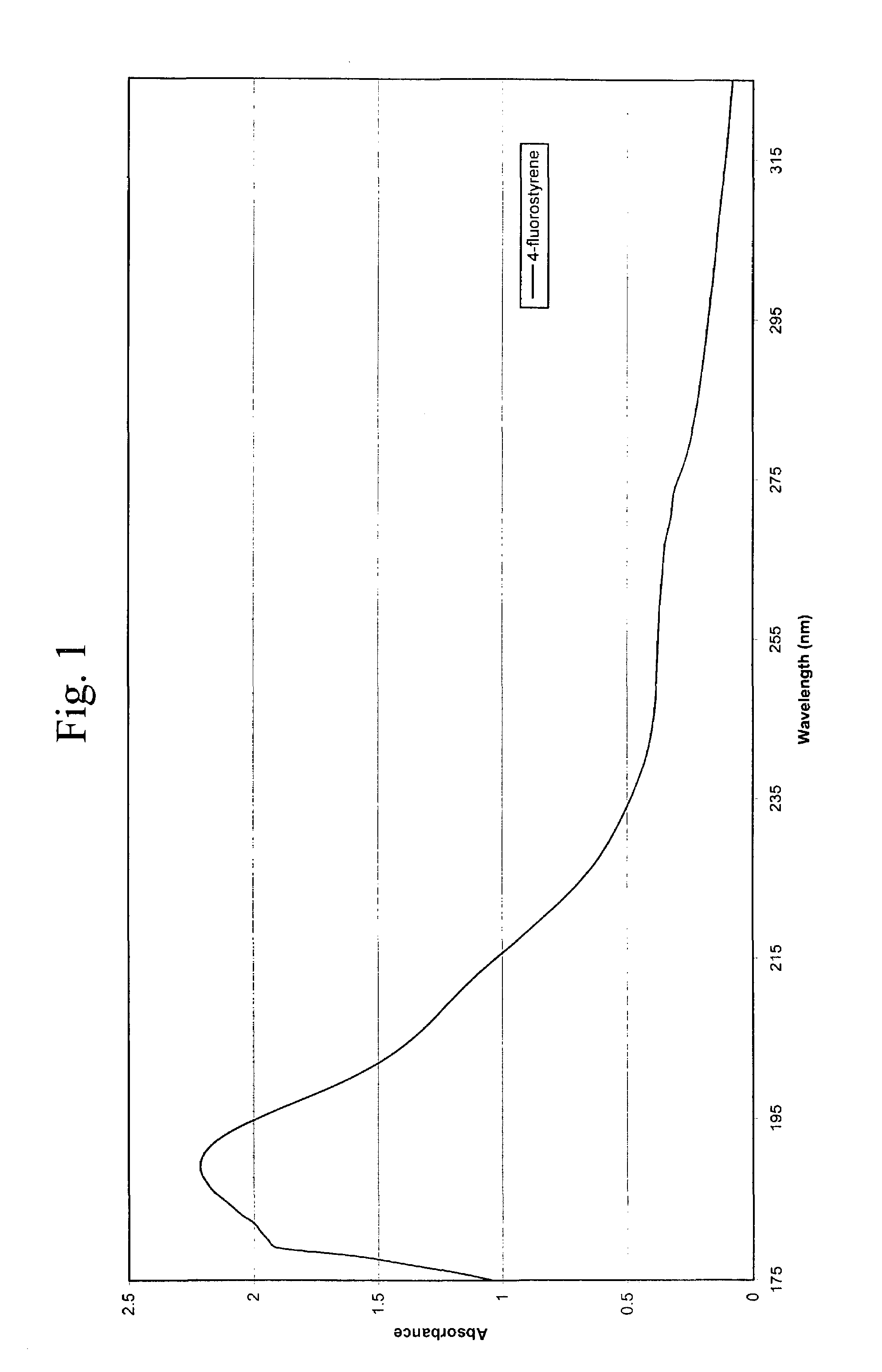
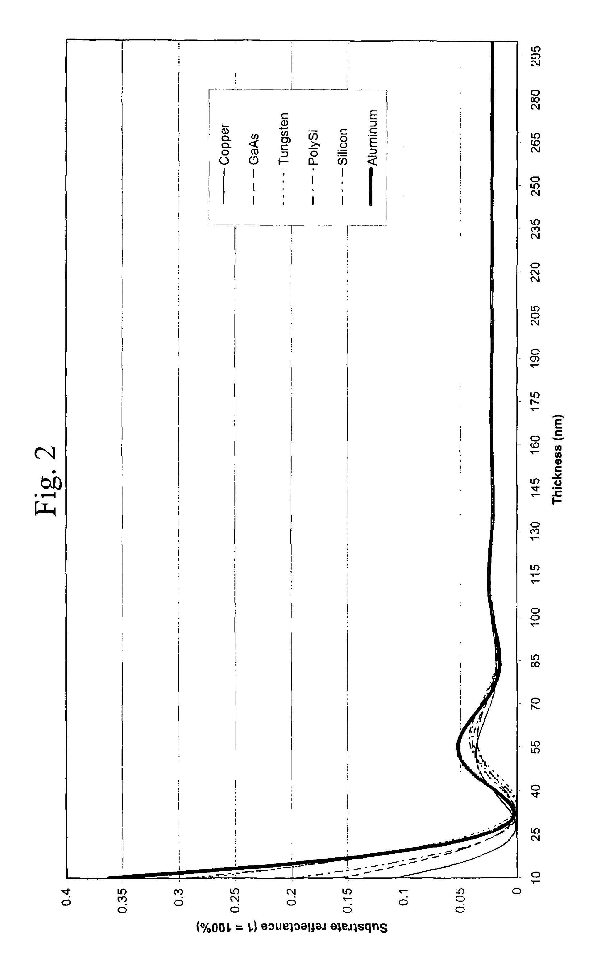
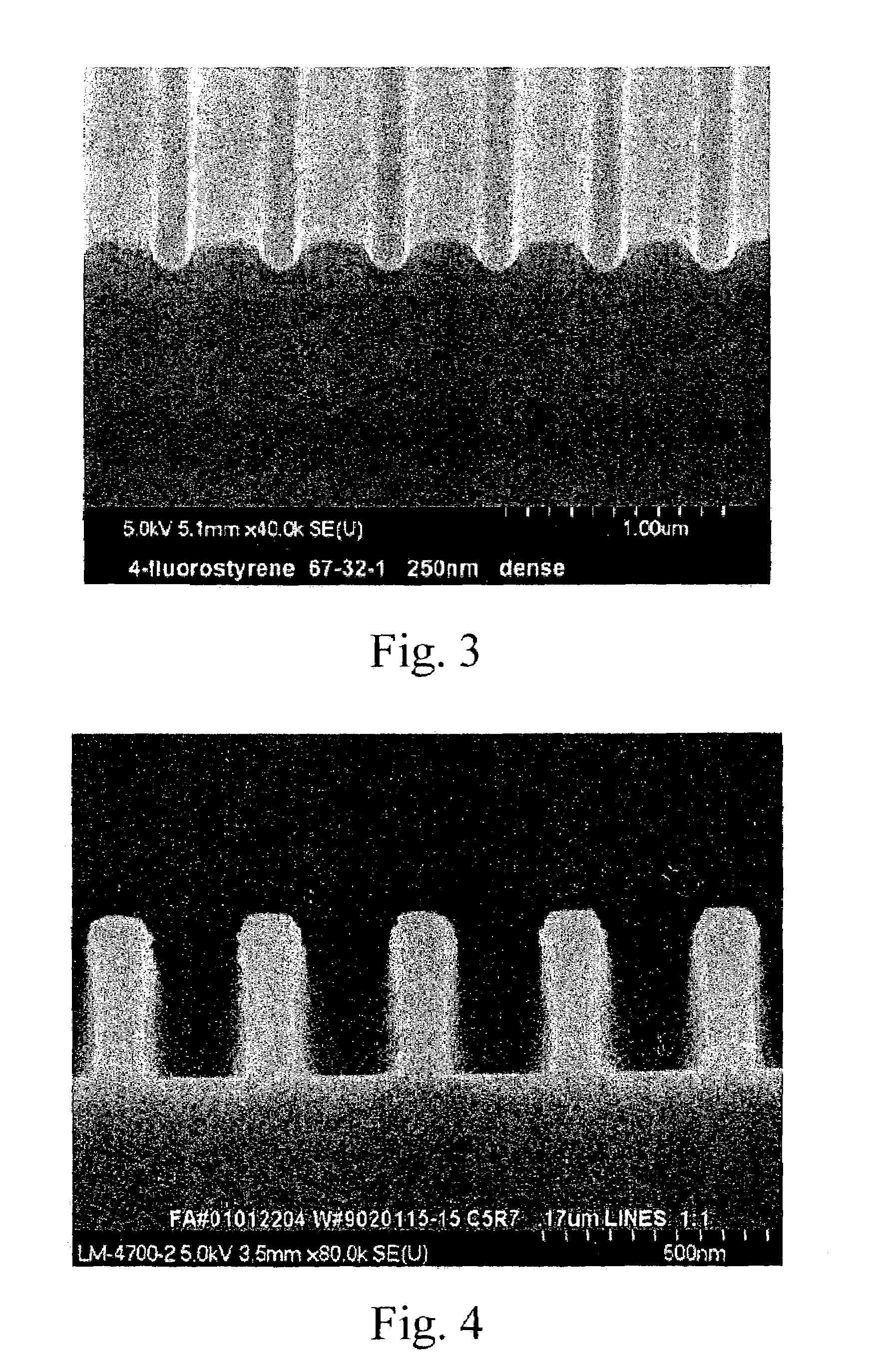
[0068]The antireflective coating layers were prepared by PECVD polymerizing a 0.2 g sample of 4-fluorostyrene (Structure A, obtained from Sigma-Aldrich) onto six- or eight-inch flat silicon wafers, topography wafers, quartz slides, aluminum substrates, tantalum (Ta) substrates, and tantalum nitride (TaN) substrates. Before deposition, the pressure was about 40 mTorr. During deposition, the pressure was maintained around 95-100 mTorr, and the temperature was room temperature (about 23° C.). The RF plasma power was set at 80 watts and cycled as discussed above. An initial eight runs on flat substrates were conducted to determine the best film thicknesses, optical properties, film uniformity, intermixing with photoresists, resistance to resist solvents, and adhesion to the various substrates. The topography wafers were used to determine conformal properties. The 4-fluorostyrene deposited at a rate of 136 Å / min. on an eight-inch substrate. This deposition ti...


PUM

PropertyMeasurementUnit
Lengthaaaaaaaaaa
Fractionaaaaaaaaaa
Pressureaaaaaaaaaa

Abstract

An improved method for applying polymeric antireflective coatings to substrate surfaces and the resulting precursor structures are provided. Broadly, the methods comprise plasma enhanced chemical vapor depositing (PECVD) a polymer on the substrate surfaces. The most preferred starting monomers are 4-fluorostyrene, 2,3,4,5,6-pentafluorostyrene, and allylpentafluorobenzene. The PECVD processes comprise subjecting the monomers to sufficient electric current and pressure so as to cause the monomers to sublime to form a vapor which is then changed to the plasma state by application of an electric current. The vaporized monomers are subsequently polymerized onto a substrate surface in a deposition chamber. The inventive methods are useful for providing highly conformal antireflective coatings on large surface substrates having super submicron (0.25 μm or smaller) features. The process provides a much faster deposition rate than conventional chemical vapor deposition (CVD) methods, is environmentally friendly, and is economical.

Description

RELATED APPLICATIONS[0001]This application claims the priority benefit of a provisional application entitled POLYMERIC ANTIREFLECTIVE COATINGS DEPOSITED BY PLASMA ENHANCED CHEMICAL VAPOR DEPOSITION, Serial No. 60 / 371,693, filed Apr. 11, 2002, incorporated by reference herein. This application is a continuation-in-part of application Ser. No. 09 / 778,980, filed Feb. 2, 2001 now abandoned, entitled POLYMERIC ANTIREFLECTIVE COATINGS DEPOSITED BY PLASMA ENHANCED CHEMICAL VAPOR DEPOSITION and incorporated by reference herein.BACKGROUND OF THE INVENTION[0002]1. Field of Invention[0003]The present invention is broadly concerned with methods of forming antireflective coating layers on silicon and dielectric materials as well as the resulting integrated circuit precursor structures. More particularly, the inventive methods comprise providing a quantity of a polymer generated by the subliming of monomers into the plasma state by electric current and subsequent polymerization thereof onto the s...

Claims


Application Information

Patent Timeline
IPC IPC(8): G03C5/00B05D3/02G03F7/11H01L21/31H01L21/469C23C14/12G02B1/11G03F7/09H01L21/027
CPCG02B1/11G03F7/091G02B1/111G03F7/11
Inventor SABNIS, RAM W.SHIH, WU-SHENGGUERRERO, DOUGLAS J.
Owner BREWER SCI
Why Eureka
Try Eureka