GaP/silicon tandem solar cell with extended temperature range

a technology of tandem solar cells and silicon, applied in the field of photovoltaic (pv) cells, can solve the problems of low efficiency of high-temperature operation, low efficiency of high-temperature techniques, and insufficient silicon to capture all available light. achieve the effect of high operating temperature, good performance and low weigh

Inactive Publication Date: 2006-12-12
NASA
View PDF16 Cites 68 Cited by
  • Summary
  • Abstract
  • Description
  • Claims
  • Application Information

AI Technical Summary

Benefits of technology

[0034]It is an object of the invention to provide a solar cell which has good performance both at temperatures around room temperature, and also at high operating temperature. Such a solar cell could be used in both high-temperature environments and also in terrestrial operating environments.
[0035]It is an object of the invention to provide a solar cell which can be manufactured on crystalline silicon (Si) substrates, because silicon is lower in weight, has greater resistance to fracture, and has higher thermal conductivity than the germanium substrates currently being used for multi-junction cells. It is also lower in cost, and is grown in larger area wafers.

Problems solved by technology

Standard silicon wafers are 200–500 μm thick, but with recently improved optical designs only 10 μm of silicon could be sufficient to capture all the available light.
It is possible to make layers from semiconductors which are not precisely matched in lattice constant, but in general this technique produces a lower quality material, and only lattice-matched (or nearly lattice-matched) materials are currently used in state-of-the-art high efficiency solar cells.
One difficulty of solar cells for some applications is that they do not operate efficiently at elevated temperatures.
At an operating temperature of 450 C, the power output is reduced to only 20% of the output at 25 C. A typical silicon solar cell has even worse temperature performance, losing about 0.45% of its initial power for each degree of increase in operating temperature.
The decrease in performance is primarily due to a decrease in voltage at the operating point.
A difficulty with this design is that Gallium Arsenide Phosphide of energy gap 1.77 to 2.09 eV is not lattice-matched to the silicon crystal, which makes growth of high quality material difficult.

Method used


Image

  • GaP/silicon tandem solar cell with extended temperature range
  • GaP/silicon tandem solar cell with extended temperature range
  • GaP/silicon tandem solar cell with extended temperature range

Examples


example 1

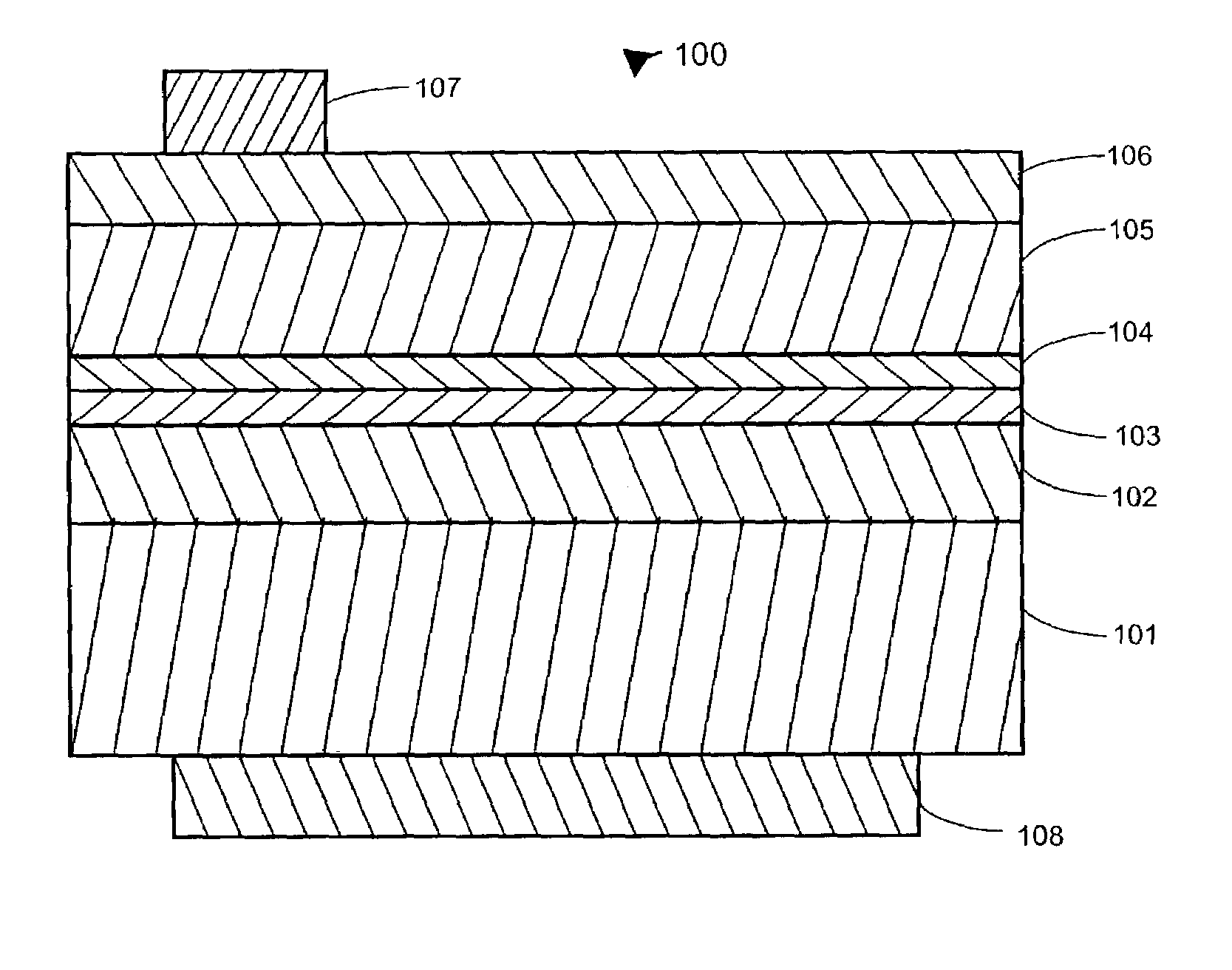
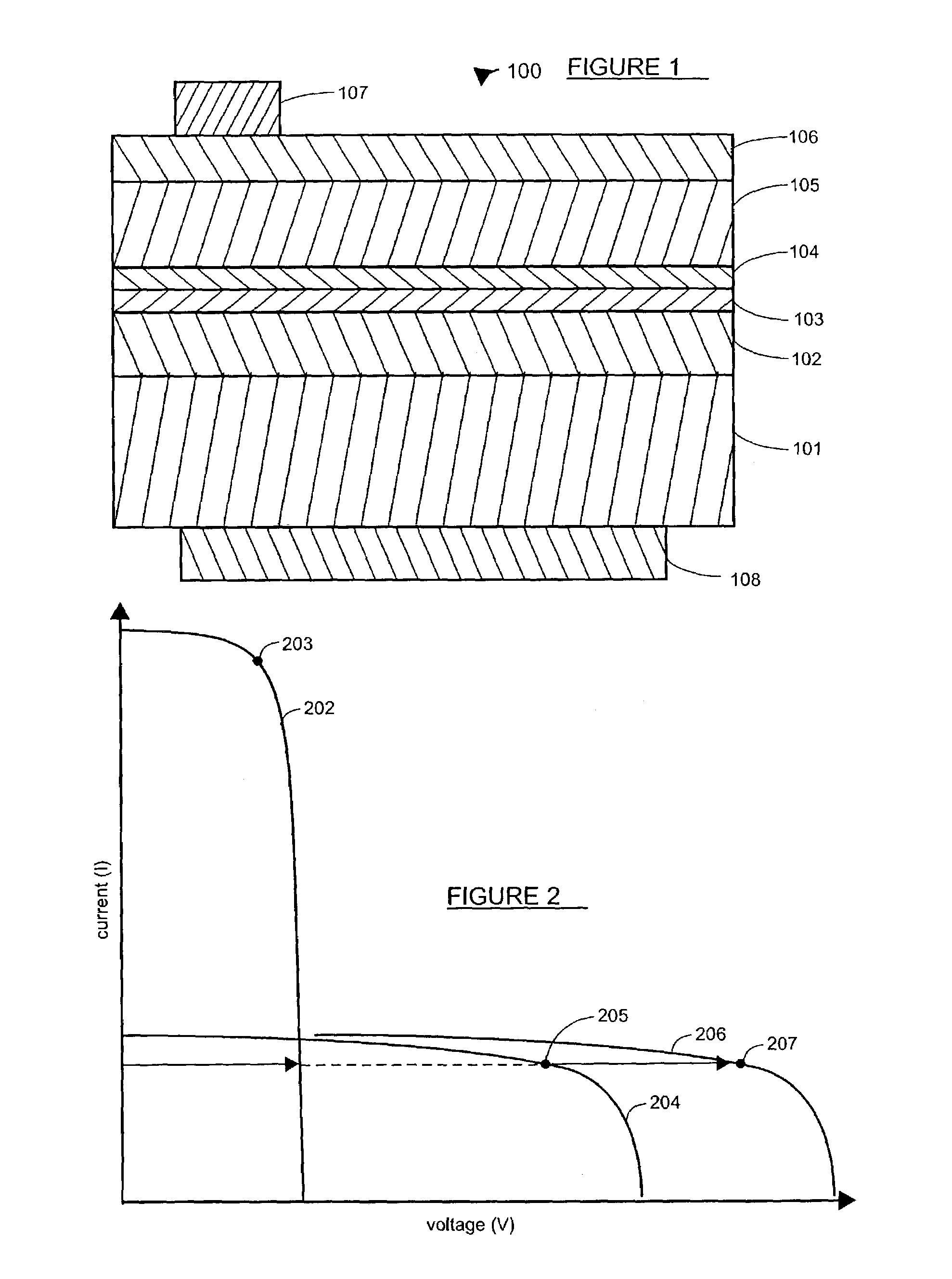
[0070]In this example, the p-n junction is disposed close to the GaP.[0071]for the substrate layer 101, a thickness of 250 micrometers, doping level p-type, 1 times ten to the fifteenth (1×10¹⁵, or 1E15) boron atoms per cubic centimeter.[0072]for the overlying layer 102, a thickness of 0.1 micrometer, doping level n-type, 1E17 phosphorous atoms per cubic centimeter.[0073]for the tunnel junction layer 103, silicon, thickness 0.05 micrometer, doping level n-type, 1E20 phosphorous atoms per cubic centimeter.[0074]for the tunnel junction layer 104, silicon, thickness 0.05 micrometer, doping level p-type, 2E20 boron atoms per cubic centimeter.[0075]for the GaP layer 105, thickness 20 micrometers, doping level p-type, 1E15 zinc atoms per cubic centimeter.[0076]for the GaP layer 106, thickness 1 micrometer, doping level n-type, 1E18 sulfur atoms per cubic centimeter.[0077]for the top metal contact 107, gold-zinc alloy (98% gold, 2% zinc)[0078]for the back metal contact 108, aluminum, thick...

example 2

[0080]In this example, the p-n junction is disposed back from the GaP.[0081]for the substrate layer 101, a thickness of 10 micrometers, doping type p-type, doping 1 times ten to the seventeenth (1E17) boron atoms per cubic centimeter.[0082]for the overlying layer 102, thickness 250 micrometers, doping type n-type, doping 1E15 phosphorus atoms per cubic centimeter.[0083]for the tunnel junction n-layer 103, silicon, thickness 0.05 micrometer, doping 1E20 phosphorus atoms per cubic centimeter.[0084]for the tunnel junction p-layer 104, silicon, thickness 0.05 micrometer, doping 2E20 boron atoms per cubic centimeter.[0085]for the GaP p-layer 105, thickness 20 micrometer, doping p-type 1E15 zinc atoms per cubic centimeter.[0086]for the GaP n-layer 106, thickness 1 micrometer, doping n-type 1E18 sulfur atoms per cubic centimeter.[0087]for the front contact metal 107, composition gold-zinc alloy (98% gold / 2% zinc).[0088]for the rear contact metal 108, composition aluminum, thickness 30 micr...


PUM


Abstract

A two-junction solar cell has a bottom solar cell junction of crystalline silicon, and a top solar cell junction of gallium phosphide. A three (or more) junction solar cell has bottom solar cell junctions of silicon, and a top solar cell junction of gallium phosphide. The resulting solar cells exhibit improved extended temperature operation.

Description

ORIGIN OF THE INVENTION[0001]The invention described herein was made by an employee of the United States Government and may be manufactured and used by or for the Government for Government purposes without the payment of any royalties thereon or therefor.TECHNICAL FIELD OF THE INVENTION[0002]The invention relates to photovoltaic (PV) cells (also known as “solar cells”) and, more particularly, to tandem (e.g., dual junction, triple junction) solar cells.BACKGROUND OF THE INVENTION[0003]It was discovered in the 1830s that exposing an electrolytic cell to light increased the amount of current it generated. But the first commercial photovoltaic (PV) products arrived only in the 1950s, when silicon PV devices produced electricity with an efficiency of 4.5 percent. By 1960, the efficiencies of research devices reached 14 percent and commercial products 10 percent.[0004]The simplest PV cell starts out as a wafer of crystal silicon, in which each atom forms covalent bonds with four adjacent...

Claims


Application Information

Patent Timeline
Patent Type & Authority Patents(United States)
IPC IPC(8): H01L31/0304
CPCH01L31/0725H01L31/03046Y02E10/50
Inventor LANDIS, GEOFFREY A.
Owner NASA
Why Eureka
Try Eureka