

Active-matrix organic electroluminescent display panel and fabricating method thereof
- Summary
- Abstract
- Description
- Claims
- Application Information
AI Technical Summary
Benefits of technology
Problems solved by technology
Method used
Image

Examples
Embodiment Construction
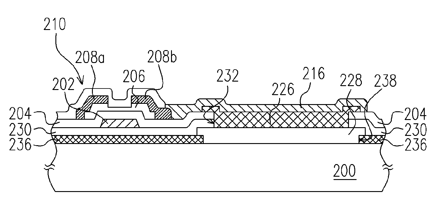
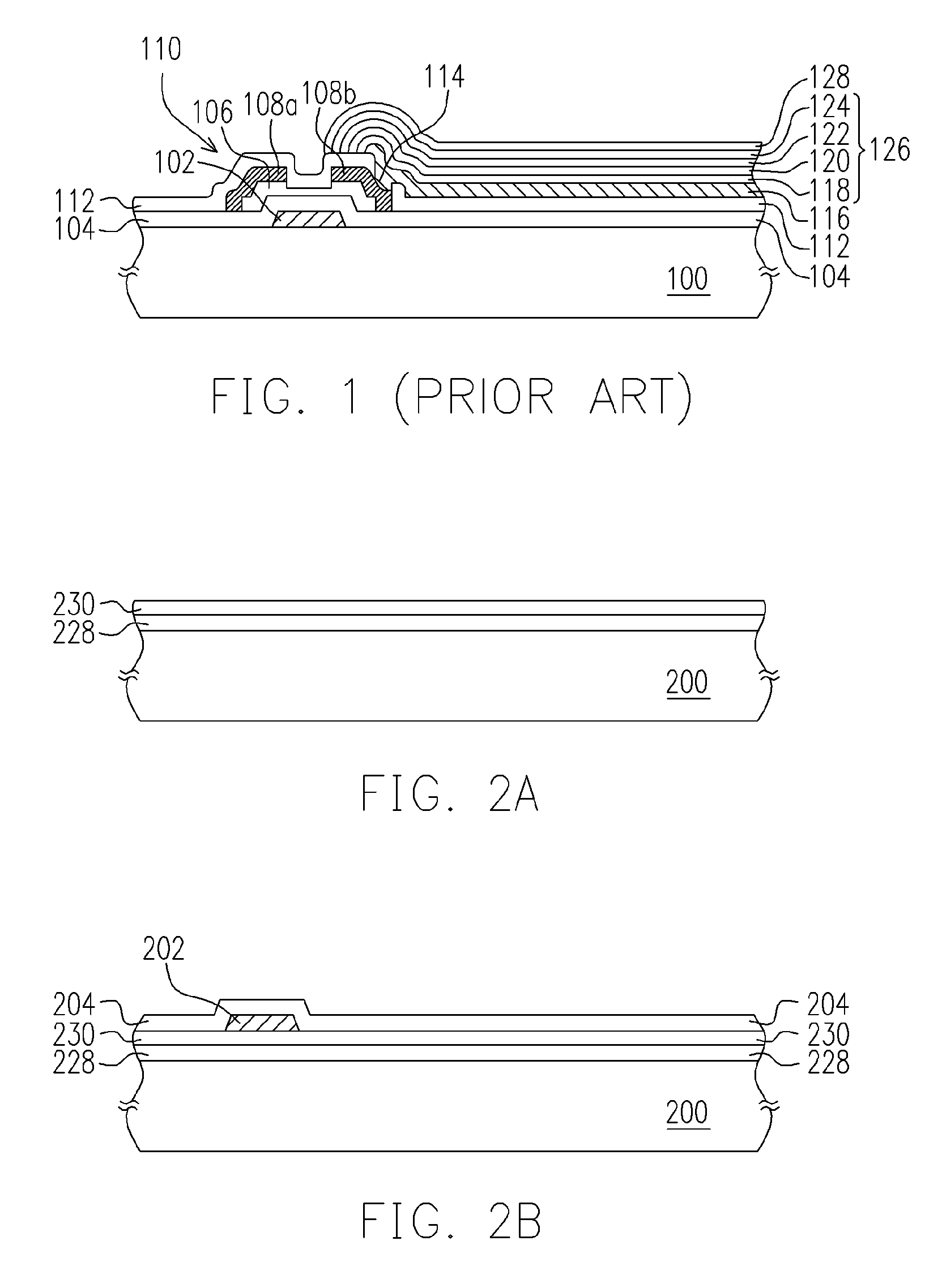
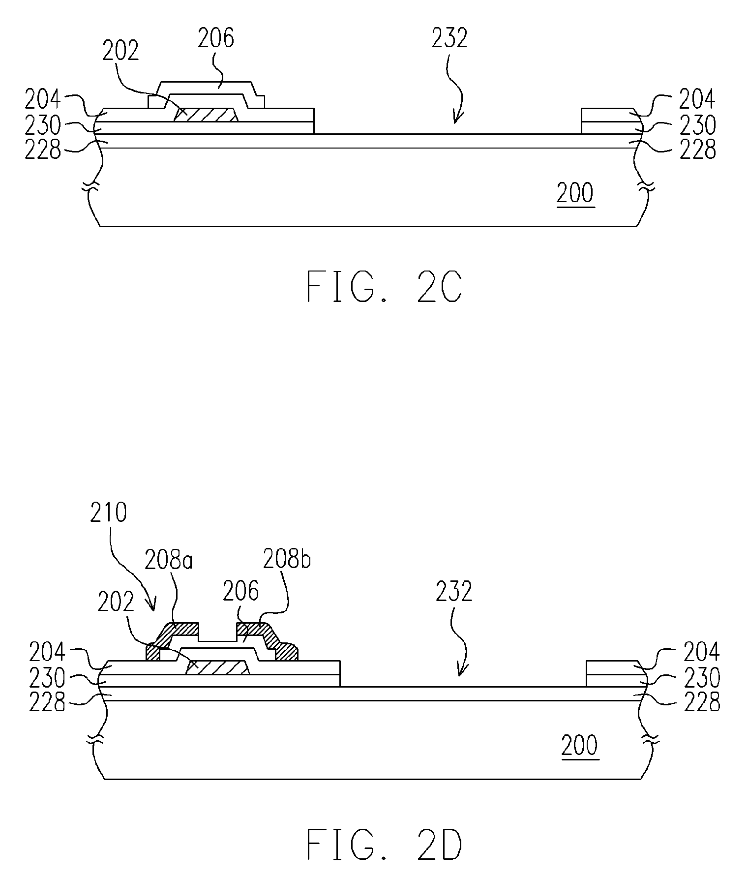
[0029]FIGS. 2A–2F illustrate a process flow of fabricating an active-matrix OEL display panel according to a preferred embodiment of this invention in a cross-sectional view. Though an OEL display panel has many OEL display elements thereon arranged as a matrix, FIGS. 2A–2F illustrate the fabrication of only one OEL display element for convenience.
[0030]Referring to FIG. 2A, a substrate 200, such as a glass substrate or a plastic substrate, is provided. A transparent conductive layer 228 is formed on the substrate 200 to serve as a common anode. The transparent conductive layer 228 includes a material such as indium tin oxide (ITO) or indium zinc oxide (IZO), and is formed with a sputtering process, for example. A blanket passivation layer 230, which includes a material such as silicon nitride, is formed on the transparent conductive layer 228 with plasma-enhanced chemical vapor deposition (PECVD), for example. The passivation layer 230 is formed to isolate the transparent conductiv...
PUM
 Abstract
Description
Claims
Application Information