Aryl amine polymer, thin film transistor using the aryl amine polymer, and method of manufacturing the thin film transistor

a technology of aryl amine polymer and thin film transistor, which is applied in the field ofaryl amine polymer, can solve the problems of difficult purification of materials, layers have a vital problem with film stability, and the state of layers changes with an extended period of time, and achieves excellent carrier mobility, high on-off ratio, and high preservability.

Active Publication Date: 2007-01-23
RICOH KK
View PDF17 Cites 38 Cited by
  • Summary
  • Abstract
  • Description
  • Claims
  • Application Information

AI Technical Summary

Benefits of technology

[0016]Another object of the present invention is to provide an organic TFT which has an excellent carrier mobility, a high-on-off ratio, a high preservability and which can achieve a printable circuit.
[0017]Another object of the present invention is to provide a method of manufacturing the organic TFT at a low manufacturing cost using a wet process (such as a spin coating method or a dipping method).

Problems solved by technology

However, in the case of layers of the low molecular weight materials, it is reported that the state of the layers changes with an extended period of time.
Therefore the layers have a vital problem with stability of the film.
However, these materials have shortcomings such as difficulty in purifying the materials and a low fluorescence quantum yield.
Currently, no high-performance light emitting device has been obtained so far.
Therefore, large cost cutting in manufacturing and large-sized devices are expected.
However, pentacene is barely soluble in a solvent and thereby forming a pentacene film from a solution is difficult.
In addition, pentacene is unstable under oxidation conditions and therefore tends to be oxidized with time in an atmosphere containing oxygen.
Similarly, materials such as phthalocyanine and fullerene are also barely soluble and generally an organic semiconductor layer thereof needs to be manufactured by a vacuum deposition method.
Therefore, advantages of the devices using organic materials such as cost cutting in manufacturing process and formability of large-sized devices cannot be expected.
Further, these materials have problems in that a film thereof tends to peel off and crack due to deformation of the substrate.

Method used


Image

  • Aryl amine polymer, thin film transistor using the aryl amine polymer, and method of manufacturing the thin film transistor
  • Aryl amine polymer, thin film transistor using the aryl amine polymer, and method of manufacturing the thin film transistor
  • Aryl amine polymer, thin film transistor using the aryl amine polymer, and method of manufacturing the thin film transistor

Examples


example 1

[0197]

[0198]A polymer 1 was prepared by: placing 0.852 g (2.70 mmol) of the dialdehyde illustrated above and 1.525 g (2.70 mmol) of the diphosphonate illustrated above in a 100 ml four-neck flask; performing nitrogen gas replacement; adding 75 ml of tetrahydrofuran to the mixture; to the solution, dropping 6.75 ml (6.75 mmol) of a tetrahydrofuran solution of 1.0 mol dm−3 of potassium t-butoxide; stirring the solution for two hours at room temperature; adding diethyl benzylphosphonate and benzaldehyde to the resultant in this order: further stirring for another two hours; adding about 1 ml of acetic acid to the resultant; after finishing the reaction, washing the solution with water; evaporating the solution to eliminate the solvent under reduced pressure; and then reprecipitating the resultant by dissolving the resultant in a tetrahydrofuran and methanol solution for purification thereof. The weight of the thus obtained polymer 1 was 1.07 g and the yield thereof was 73%.

[0199]Elemen...

example 2

[0203]

[0204]A polymer 2 was prepared in the same manner as illustrated in Example 1 using 419.5 mg (1.00 mmol) of the dialdehyde illustrated above and 564.5 mg (1.00 mmol) of the diphosphonate illustrated above. The amount of the thus obtained polymer 2 was 518.3 mg and the yield thereof was 62%.

[0205]Elemental analysis value (theoretical value): C 85.18%; (85.55%), H 8.03%; (7.63%), N 2.10%; (2.08%).

[0206]The Glass transition temperature of the polymer 2 obtained using differential scanning calorimetry (DSC) was 133° C.

[0207]The polystyrene-conversion number average molecular weight and weight average molecular weight measured by gel permeation chromatography (GPC) were 39,200 and 116,000, respectively.

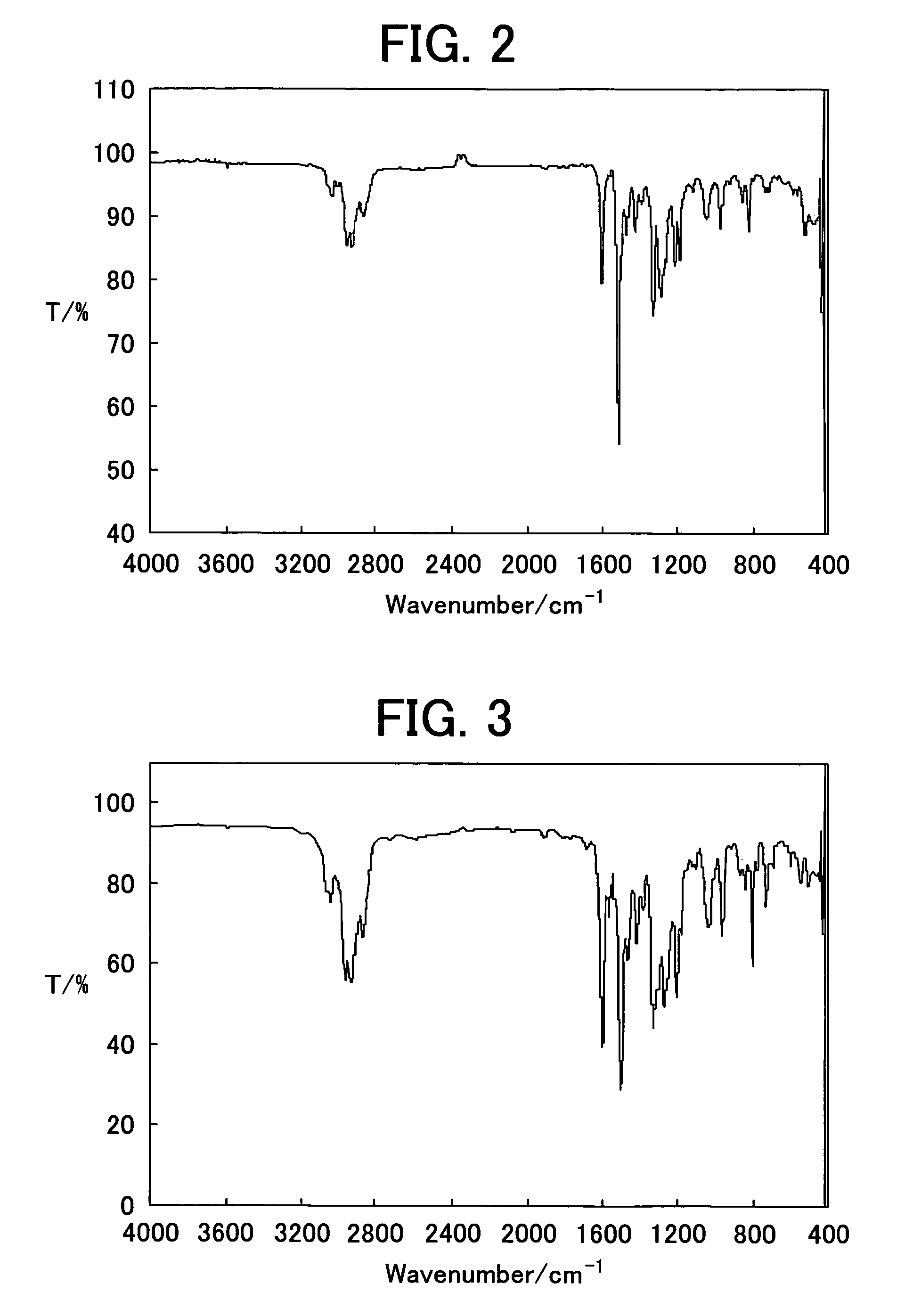
[0208]Infrared absorption spectrum (NaCl cast film) of the polymer 2 is shown in FIG. 3.

example 3

[0209]

[0210]A polymer 3 was prepared in the same manner as illustrated in Example 1 using 1.00 g (2.40 mmol) of the dialdehyde illustrated above and 1.35 g (2.40 mmol) of the diphosphonate illustrated above. The amount of the thus obtained Polymer 3 was 1.32 g and the yield thereof was 82%.

[0211]Elemental analysis value (thoretical value): C 85.33%; (85.55%), H 7.86%; (7.63%), N 2.30%; (2.08%).

[0212]The glass transition temperature of the polymer 3 obtained using differential scanning calorimetry (DSC) was 151.9° C.

[0213]The polystyrene-conversion number average molecular weight and weight average molecular weight measured by gel permeation chromatography (GPC) were 44,400 and 118,000, respectively.

[0214]Infrared absorption spectrum (NaCl cast film) of the polymer 3 is shown in FIG. 4.


PUM

PropertyMeasurementUnit
surface energyaaaaaaaaaa
surface roughnessaaaaaaaaaa
temperatureaaaaaaaaaa

Abstract

An aryl amine polymer is provided which contains a specific repeat unit, its use in preparing an organic semiconductor material which contains the aryl amine polymer and an additional specific compound and in the preparation of organic light emitting devices (OLED), organic thin film transistors (TFT) and so on, along with an organic TFT including a substrate, an organic semiconductor layer which contains the organic semiconductor material and is located overlying the substrate, an electrode pair of a source electrode and a drain electrode; and a third electrode.

Description

FIELD OF THE INVENTION[0001]The present invention relates to an aryl amine polymer for organic light emitting devices, organic transistors and so on. Also the present invention relates to an organic thin film transistor (TFT) using the aryl amine polymer as a semiconductor layer therein and a method of manufacturing the organic TFT.DISCUSSION OF THE BACKGROUND[0002]Organic light emitting devices and organic transistor devices have been proposed utilizing various characteristics of organic materials such as light emitting and charge transport characteristics. By using organic materials for these devices, advantages such as light weight, low price, low manufacturing cost and flexibility are expected.[0003]For materials for use in organic light emitting devices, various materials from low molecular weight materials to polymeric materials have been reported. As for low molecular weight materials, it is reported that efficiency is boosted by adopting various kinds of layer structures and...

Claims


Application Information

Patent Timeline
Patent Type & Authority Patents(United States)
IPC IPC(8): C08G73/00C08G61/12C08G83/00H01L29/72H01L51/00H01L51/05H01L51/30H01L51/50
CPCC08G61/12C08G73/00H01L51/0035H01L51/0038Y02E10/549H01L51/0541H01L51/0545H01L51/5048Y10S428/917H01L51/0043Y02P70/50H10K85/114H10K85/111H10K85/151H10K10/464H10K10/466H10K50/14
Inventor SAGISAKA, TOSHIYASASAKI, MASAOMITORII, MASAFUMIKAWAMURA, SHINICHIOKADA, TAKASHINAKAYAMA, YOSHINOBUAKIYAMA, YOSHIKAZUKONDOH, HITOSHITOMONO, HIDENORIYAMAGA, TAKUMI
Owner RICOH KK
Why Eureka
Try Eureka