Selective metal encapsulation schemes

Inactive Publication Date: 2007-04-17
APPLIED MATERIALS INC
View PDF446 Cites 38 Cited by
  • Summary
  • Abstract
  • Description
  • Claims
  • Application Information

AI Technical Summary

Benefits of technology

[0014]The methods and systems of the present invention provide a semiconductor device having a conductive element selectively encapsulated by a metallic passivating layer. The passivating layer interface with the conductive element is of low capacitance. The passivating layer also provides an effective barri

Problems solved by technology
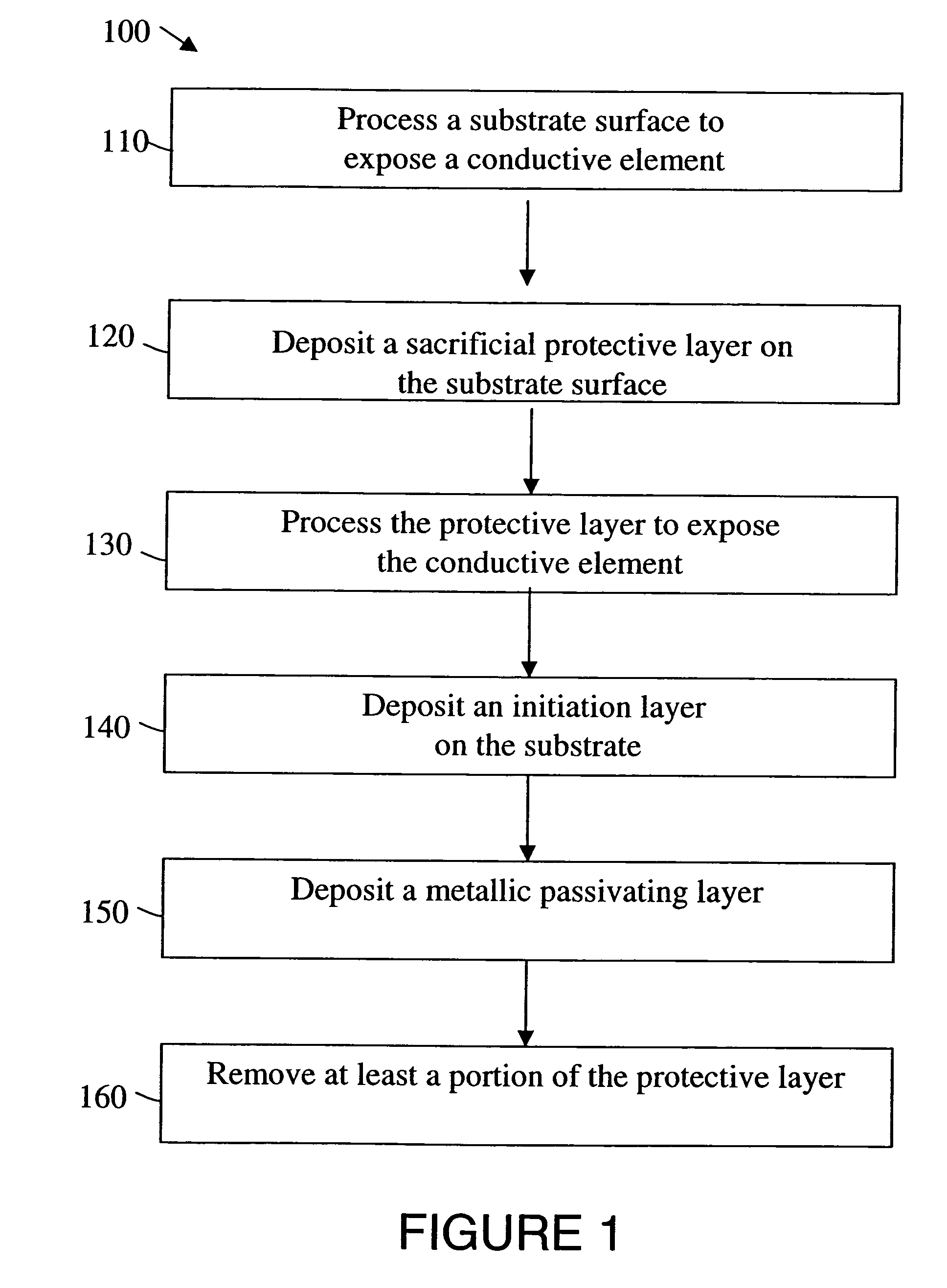
However, copper readily forms copper oxide when exposed to atmospheric conditions or environments outside of processing equipment.
Metal oxides can result in an increase the resistance of metal layers, become a source of particle problems, and reduce the reliability of the overall circuit.
Furthermore, the electromigration of copper in dielectric materials is unacceptably high.
However, copper does not satisfactorily catalyze or initiate deposition of materials from electroless solutions.
However, deposition of the catalytic material may require multiple steps or the use catalytic colloidal compounds.
Catalytic colloidal compounds, and colloidal palladium materials in particular, adhere to dielectric materials and result in the undesir

Method used


Image

  • Selective metal encapsulation schemes
  • Selective metal encapsulation schemes
  • Selective metal encapsulation schemes

Examples


Example

[0020]The words and phrases used herein should be given their ordinary and customary meaning in the art by one skilled in the art unless otherwise further defined.

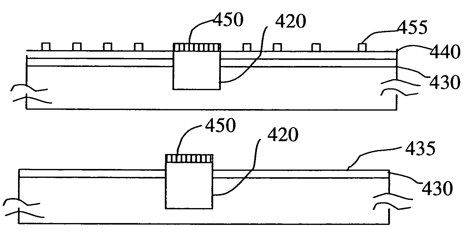
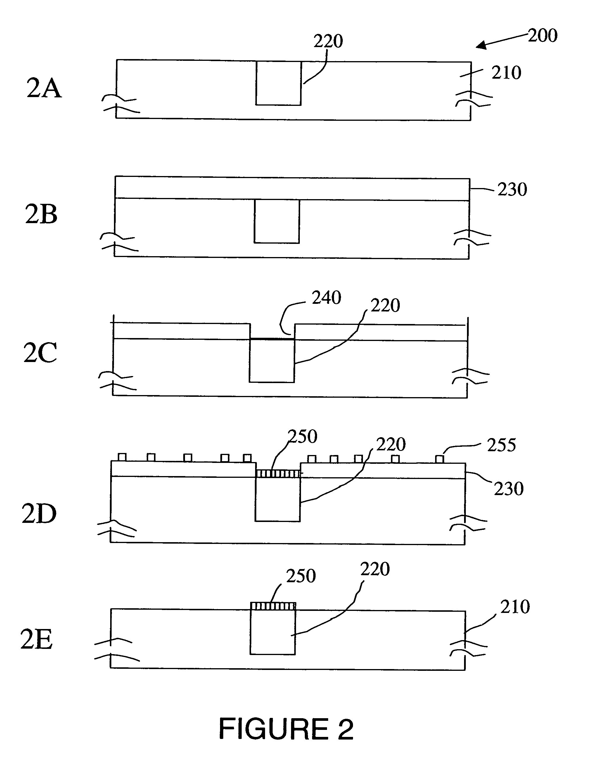
[0021]“Substrate surface” as used herein refers to a layer of material that serves as a basis for subsequent processing operations. For example, a substrate surface may contain one or more “conductive elements,” such as aluminum, copper, tungsten, or combinations thereof, and may form part of an interconnect feature such as a plug, via, contact, line, wire, and may also form part of a metal gate electrode. A substrate surface may also contain one or more nonconductive materials, such as silicon, doped silicon, germanium, gallium arsenide, glass, and sapphire. The substrate surface may also contain one or more low k materials such as carbon-doped oxides, porous low k materials such as organic low k and inorganic low k materials and hybrids thereof, or air-gap structures.

[0022]The term “about” is used herein to mean approxim...


PUM


Abstract

A method and system of processing a semiconductor substrate includes, in one or more embodiments, depositing a protective layer on the substrate surface comprising a conductive element disposed in a dielectric material; processing the protective layer to expose the conductive element; electrolessly depositing a metallic passivating layer onto the conductive element; and removing at least a portion of the protective layer from the substrate after electroless deposition. In another aspect, a method and system of processing a semiconductor includes depositing a metallic passivating layer onto a substrate surface comprising a conductive element, masking the passivating layer to protect the underlying conductive element of the substrate surface, removing the unmasked passivating layer, and removing the mask from the passivating layer.

Description

RELATED APPLICATIONS[0001]This application claims priority under 35 U.S.C. § 119(e) to U.S. provisional application Ser. No. 60 / 475,351, filed Jun. 3, 2003, which is incorporated herein by reference.FIELD OF THE INVENTION[0002]The present invention relates generally to semiconductor manufacturing, and more particularly to systems and methods for the deposition of barrier film layers on a conductive feature of the device.BACKGROUND OF THE INVENTION[0003]A common goal in the integrated circuit (IC) industry is to place more conductive circuitry into a smaller substrate surface area. Recent improvements in circuitry of ultra-large scale integration (ULSI) on semiconductor substrates indicate that future generations of semiconductor devices will require sub-quarter micron (or less) multilevel metallization. The multilevel interconnects that lie at the heart of this technology require planarization of interconnect features formed in high aspect ratio apertures, including contacts, vias, ...

Claims


Application Information

Patent Timeline
IPC IPC(8): H01L21/44H01L21/288H01L21/4763H01L21/66H01L21/768
CPCH01L21/288H01L21/76829H01L21/76849H01L21/7685H01L21/76885
Inventor PADHI, DEENESHGANDIKOTA, SRINIVASNAIK, MEHULPARIKH, SUKETU A.DIXIT, GIRISH A.
Owner APPLIED MATERIALS INC
Why Eureka
Try Eureka