Electromagnetic wave absorption material and an associated device

a technology of electromagnetic wave absorption and electromagnetic wave, which is applied in the field of new electromagnetic wave absorption materials, can solve the problems of preventing the realization of light-weight electromagnetic wave absorbers, malfunctioning problems, and devices that easily emit undesired noise, and achieves excellent radio wave absorption performance, easy manufacturing, and light weight

Inactive Publication Date: 2007-07-03
HITACHI LTD
View PDF19 Cites 41 Cited by
  • Summary
  • Abstract
  • Description
  • Claims
  • Application Information

AI Technical Summary

Benefits of technology

[0012]The purpose of the present invention is to provide an electromagnetic wave absorption material having an excellent radio wave absorbing performance usable spanning from sub-millimeter wave region to millimeter wave region in which radio wave frequency ranges from 1 to 300 GHz, and the one being easy to manufacture and light in weight. The purpose further includes to provide various appliances of and systems with said electromagnetic wave absorption material particularly an electronic device, an optical transmission or reception module, a high frequency telecommunication equipment, and a stop-free tollgate system which is prevented from malfunctioning due to electromagnetic wave interference.
[0013]The inventors of the present invention found that an electromagnetic wave absorption material comprised of a dispersions of multi-layer hollow globule of carbon mixed into electrical insulating organic material has a far more excellent performance as the electromagnetic wave absorption material available for use in millimeter wave region compared to an electromagnetic wave absorbing material relying on dielectric loss, i.e. a dispersions of carbon-based substance, such as carbon black particulate, graphite, coke, carbon microcoil, and carbon nanotube, mixed into electrical insulating organic material like rubber and resin. Since said multi-layer hollow globule of carbon or a multi-layer hollow globule of carbon existing in a natural schungite ore (hereinafter referred to as a schungite carbon) is contained in natural schungite ore, the use such material for the electromagnetic wave absorption material sees little difficulty. Particularly, the present invention is devised based on the finding that such globule has a high absorption property in millimeter wave region of which frequencies are 30 to 300 GHz.
[0017]The electromagnetic wave absorption material in the present invention prefers a configuration wherein content of the multi-layer hollow globule or the schungite carbon is graded to plural degrees so that characteristic impedance may reduce toward inside from the incident plane of electromagnetic wave. Thereby, the electromagnetic wave absorbing performance for an oblique incidence of electromagnetic wave is improved or becomes being capable of accommodating electromagnetic wave of wide range of frequencies.
[0018]Material having a high electrical resistivity can contain at least one of: a magnetic metal of which main constituent is at least one of iron (Fe), cobalt (Co), and nickel (Ni); a compound selected from the group consisting of an oxide, a nitride, and a carbide, in which their main constitution is at least one of iron (Fe), cobalt (Co), nickel (Ni), aluminum (Al), silicon (Si), titanium (Ti), barium (Ba), manganese (Mn), zinc (Zn), and magnesium (Mg); and a carbon-based substance which contains at least one of carbon black, graphite, coke, and carbon microcoil. Thereby the absorbing performance of the electromagnetic wave absorption material is more improved.
[0027]According to the present invention, it is practicable to provide an economical electromagnetic wave absorption material having far more excellent performance in absorbing property than that in a dielectric loss type electromagnetic wave absorbing material in the prior art comprised of carbon-based material.
[0028]Further according to the present invention, electromagnetic wave interference within an electronic device is efficiently suppressed by use of a light weight electromagnetic wave absorption material having an absorbing property usable from submillimeter wave region to millimeter wave region. Thus, it becomes practicable to provide equipment acceptable for use in a high speed telecommunication network, such as semiconductor device, an optical transmission module, an optical reception module, or an optical transmission-reception module, and high frequency telecommunication equipment; thanks to their capability rendered from the absorbing material of suppressing internal noise interference and noise emission to outside, of achieving small-sizing and weight-reduction, of working under high speed transmission, and of having high sensitivity. Moreover according to the present invention, it also becomes practicable to provide an automated tollgate capable of exchanging information between a roadside communication equipment and an on-vehicle equipment free from suffering electromagnetic wave interference.

Problems solved by technology

This raised frequency allows such devices to easily emit undesired noise.
At the same time, narrowed noise margin in the recent electronic device because of lowered power consumption therein, together with poor quality in noise-ambient inside an apparatus because of miniaturization and dense mounting in the electronic device, brings a malfunctioning problem due to EMI (Electro-Magnetic Interference)
However, such magnetic material prevents realization of light-weight electromagnetic wave absorber because of its inherent weightiness.
However, said magnetic material is still unsatisfactory in its electromagnetic wave absorption performance.
Although the electromagnetic wave absorption material according to said Japanese Patent application laid-open No. 2001-358493 is satisfactory for sub-millimeter wave region up to 5.8 GHZ, the use in the millimeter wave region over such frequency does not satisfy with the performance of said material.

Method used


Image

  • Electromagnetic wave absorption material and an associated device
  • Electromagnetic wave absorption material and an associated device
  • Electromagnetic wave absorption material and an associated device

Examples


embodiment 1

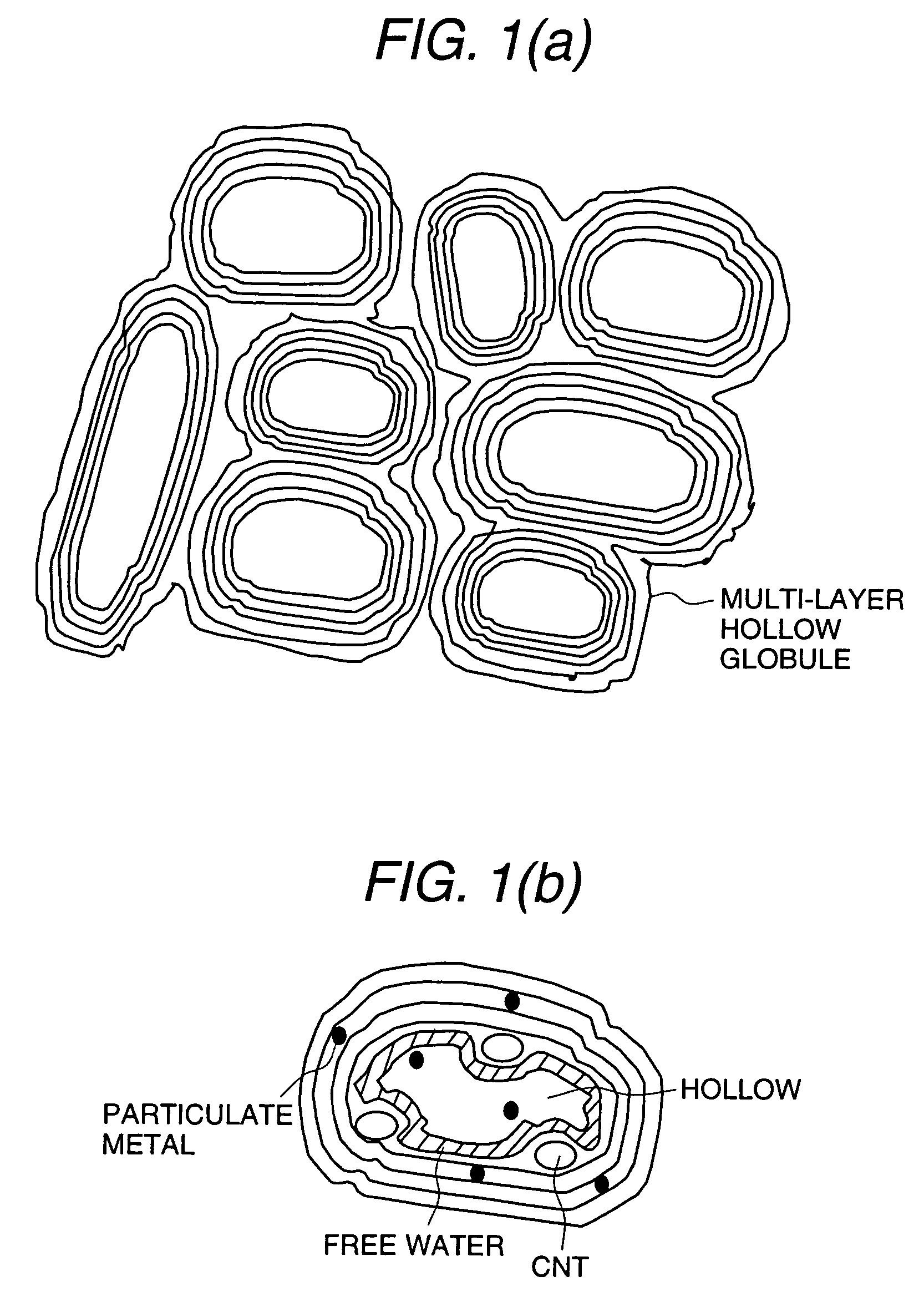
[0043]FIG. 1 is a pattern diagram of the schungite carbon, being contained in a natural schungite ore, which is composed of a multi-layer small hollow sphere of carbon called a globule. As shown in FIG. 1(b), the globule contains, inside thereof, a small quantity of a carbon nanotube (CNT), metals (Cu, Ni, V, Cr, Co, Mn, and Ti), and free water. These metals exist there in a form of silicate, sulfide, and oxide. The natural schungite ore contains 28 to 32% of the schungite carbon in weight ratio together with 57 to 66% of SiO2, 3 to 5% of Al2 O3, 1 to 3% of Fe2O3 +FeO, 0.5 to 2% of K2O, 0.2 to 1.0% of sulfur, 0.2˜0.5% of free water, and 0.3% or less for the lump of TiO2, MgO, CaO, Na2O, and MnO.

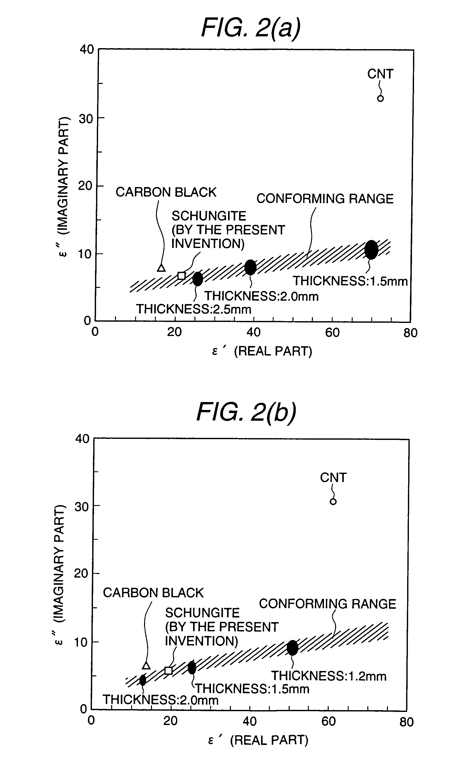
[0044]FIG. 2 graphs the relative dielectric constant of the sheet-shaped electromagnetic wave absorption material for a range of frequencies. Said sheet of absorbing material was prepared using: a carbon black (hereinafter abbreviated to CB) and a carbon nanotube (hereinafter abbreviated to C...

embodiment 2

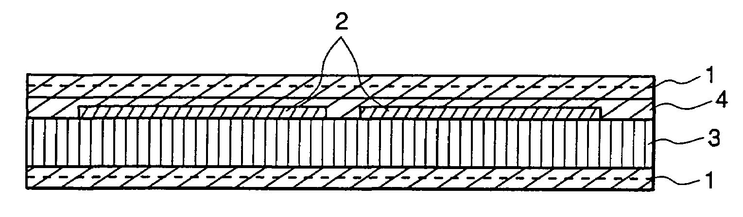
[0058]FIG. 5 is a cross sectional view of the printed wiring board equipped with an electromagnetic wave absorbing layer comprised of the electromagnetic wave absorption material by the present invention. A printed wiring board 3 comprised of a circuit wiring 2 formed on an insulator board has an insulting layer 4 on its one side of surface where said circuit wiring 2 is formed; and the other side, the reverse side thereto, has no wiring. On a part of said insulating layer 4 and on a part of said reverse side, or all of the both, a material comprised of ground powder of the natural schungite ore and a binder resin is applied to provide an electromagnetic wave absorbing layer thereon. This application is performed either by a direct coating of painting of said material or by providing a sheet of said material. The thickness of said coating or sheet is preferred to be 0.1 to 1.0 mm, though it may be designed otherwise depending on the frequency generated and the absorbing rate for ele...

embodiment 3

[0059]FIG. 6 is a cross sectional view of the electromagnetic wave absorbing cap for semiconductors arranged on a printed wiring board so that a semiconductor element that will generate noises may be enveloped thereby. This is to show a configuration of an arrangement of an electromagnetic wave absorbing cap, to which the present invention concerns, that is placed on a printed wiring board so that a possible noise generating source, such as a microprocessor or a system LSI, may be enveloped by said cap. FIG. 6(a) shows a configuration in which the electromagnetic wave absorbing layer by the present invention is arranged inside a metal cap 5 for shielding against electromagnetic wave coming from outside and for absorbing electromagnetic wave emitted from inside. The metal cap 5 uses copper plated material, copper and gold plated material, or stainless steel. FIG. 6(b) show a cap made by injection molding using electromagnetic wave absorption material by the present invention. An elec...


PUM

PropertyMeasurementUnit
frequencyaaaaaaaaaa
frequenciesaaaaaaaaaa
weight ratioaaaaaaaaaa

Abstract

The purpose of the present invention is to provide an easy-to-manufacture electromagnetic wave absorption material usable from submillimeter wave region to millimeter wave region with an excellent radio wave absorbing performance and a variety of usage thereof.The present invention is characterized by an electromagnetic wave absorption material comprised of a dispersions of at least one of the materials: a multi-layer hollow globule of carbon, a schungite carbon, and the schungite ore; mixed into a matter having a high electrical resistivity. The invention is further characterized by an electronic device, an optical transmission module, an optical reception module, a high frequency telecommunication equipment, and a stop-free automated tollgate system, wherein at least a part of their board, electronic element, and circuit wiring are covered with said electromagnetic wave absorption material.

Description

[0001]This is a continuation of application Ser. No. 10 / 235,711 filed Sep. 6, 2002 now U.S. Pat. No. 6,818,821.BACKGROUND OF THE INVENTION[0002]1. Field of the Invention[0003]The present invention relates to a novel electromagnetic wave absorption material and associated devices. The invention relates to various articles particularly, such as, an electromagnetic wave absorption material for millimeter wave of 1 to 300 GHz band, a printed wiring board that uses such absorbing material, an electronic device, a casing for an electronic device, a module for optical transmission or reception, automated tollgate, and high frequency communication equipment.[0004]2. Description of the Prior Art[0005]In late years, the high speed processing in electronic devices is spreading at an accelerating pace together with rapidly raised operating frequency of ICs and LSIs in microprocessors. This raised frequency allows such devices to easily emit undesired noise.[0006]Moreover, in the telecommunicati...

Claims


Application Information

Patent Timeline
Patent Type & Authority Patents(United States)
IPC IPC(8): H01Q17/00H05K9/00H05K1/02H05K3/28
CPCB82Y10/00B82Y30/00H05K9/0024H05K9/0083H01L2924/1423Y10S977/932H01L2924/12041H01L2224/16225H01L2224/48091H01L2224/48227H01L2924/01012H01L2924/01025H01L2924/01046H01L2924/01078H01L2924/01079H01L2924/16152H01L2924/3011H01L2924/3025H05K3/284H01L2924/00014H01L2924/00H01Q17/004H05K9/0029H05K9/0031C01B32/05H05K9/00
Inventor FUJIEDA, TADASHIHIDAKA, KISHIOIKEDA, SHINZOUHAYASHIBARA, MITSUOTAGUCHI, NORIYUKI
Owner HITACHI LTD
Why Eureka
Try Eureka