Grinding abrasive grains, abrasive, abrasive solution, abrasive solution preparation method, grinding method, and semiconductor device fabrication method

a technology of grinding abrasives and grains, which is applied in the direction of lapping machines, manufacturing tools, other chemical processes, etc., can solve the problems of affecting the quality of wafers, the grinding speed of abrasives is not necessarily faster, and many errors, etc., to achieve high-speed grinding, poor mechanical strength, and strong cleavage

Active Publication Date: 2007-09-11
SUMITOMO CHEM CO LTD
View PDF10 Cites 24 Cited by
  • Summary
  • Abstract
  • Description
  • Claims
  • Application Information

AI Technical Summary

Benefits of technology

[0051]The invention can provide an excellent-shape wafer without peripheral dripping, while realizing high-speed grinding. Also, the invention is suitable for grinding wafers having a poor mechanical strength and a strong cleavage.

Problems solved by technology

In the grinding step of a wafer fabrication process, there are many problems of removing shape irregularities, removing thickness variations, removing machining strains, adjusting flatness, etc.
In general, combined chemical and mechanical grinding is applied to the grinding step, and abrasive is a consumable item which largely affects wafer quality.
Even though abrasive grains are amorphous, however, its grinding speed is not necessarily faster.
Also, when abrasive grains are observed with an electron microscope, unlike a dispersed state in an actual solution, tertiary grains consisting of a plurality of aggregated secondary grains or quaternary grains consisting of a plurality of aggregated tertiary grains are observed, which causes many errors, and are not efficient.
In this case, however, added metal ions are an impurity which adversely affects a wafer surface.
However, control of grain size and secondary grain shape is difficult, and stable grinding characteristics cannot be obtained, which results in no effect on some objects to be ground.
It describes use of polyaluminum chloride as the flocculent, however, such added metals are a kind of impurities, which results in a contaminated wafer surface to be ground.
Large problems with the primary grinding step lie in ensuring a wafer shape is of a stable precision, and realizing high-speed grinding.
In particular, wafer shape is important, where failure to ensure a wafer shape with a stable precision would affect the subsequent secondary grinding step.
The secondary grinding step is the mirror finish step by smoothing wafer surface roughness, often using an abrasive without abrasive grains, which results in no shape correction capability.
In particular, a soft abrasive pad of a nonwoven cloth or a suede type typically tends to cause peripheral dripping in the wafer, compared to a abrasive pad made of foamed polyurethane used in CMP (Chemical Mechanical Polishing), which results in difficulty in obtaining good flatness.
Also, there is the large problem that the above soft abrasive pad degrades fast, grinding characteristics changing with the degradation of the abrasive pad, which results in more remarkable peripheral dripping in a wafer peripheral portion.
As a method for improving malfunction caused by the abrasive pad, there is the method for improving flatness by increasing the elasticity of the abrasive pad, but using this would rather increase the incidence of flaws.
On the other hand, in the research and development of abrasives, as described in the above patent references, various researches have been made on grinding speed, surface roughness, and the reduction of defects (e.g., flaws), but as it stands, there are no disclosures about techniques for enhancing flatness by preventing peripheral dripping, or enhancing wafer shape stability over time.

Method used


Image

  • Grinding abrasive grains, abrasive, abrasive solution, abrasive solution preparation method, grinding method, and semiconductor device fabrication method
  • Grinding abrasive grains, abrasive, abrasive solution, abrasive solution preparation method, grinding method, and semiconductor device fabrication method
  • Grinding abrasive grains, abrasive, abrasive solution, abrasive solution preparation method, grinding method, and semiconductor device fabrication method

Examples


example 1

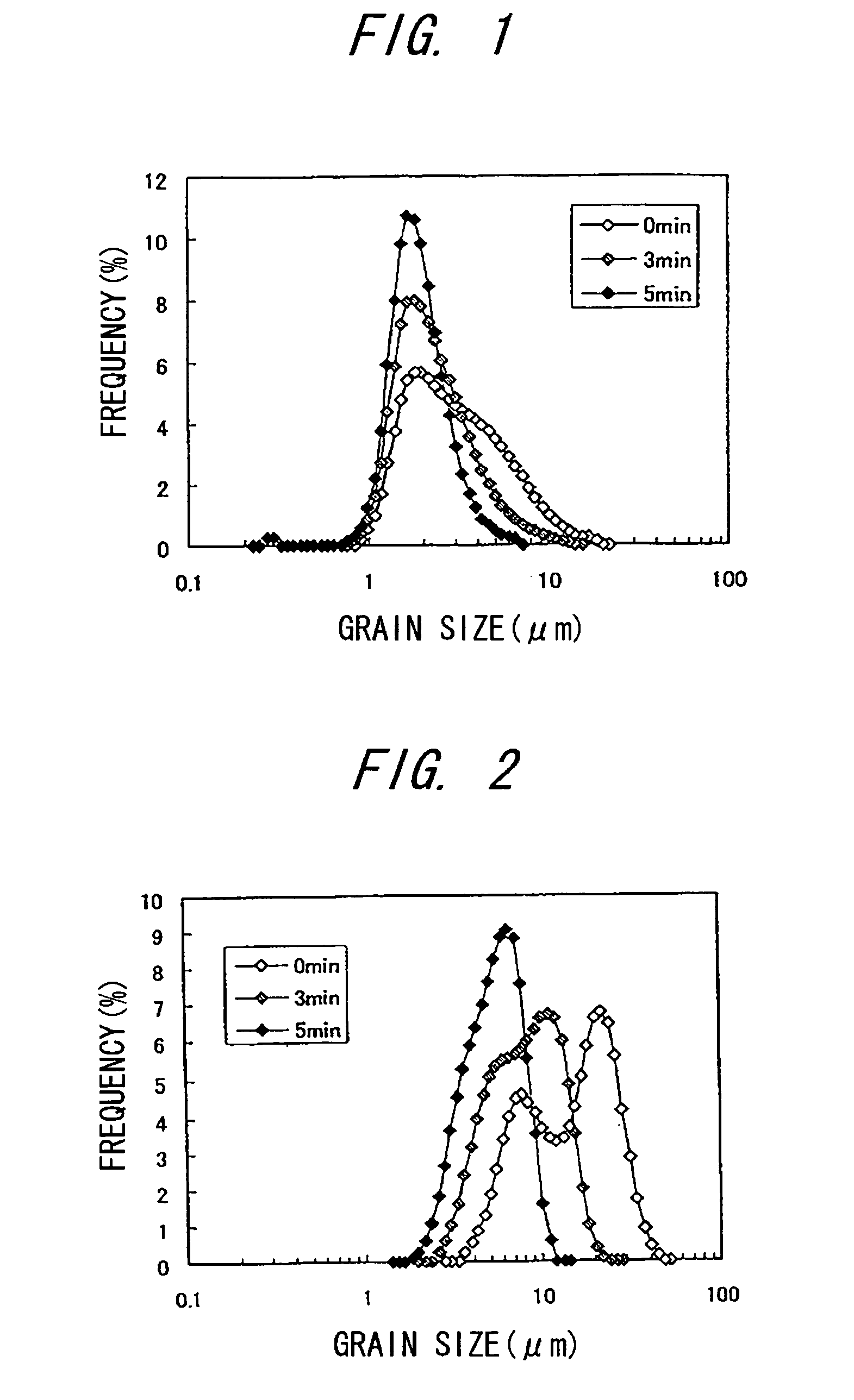
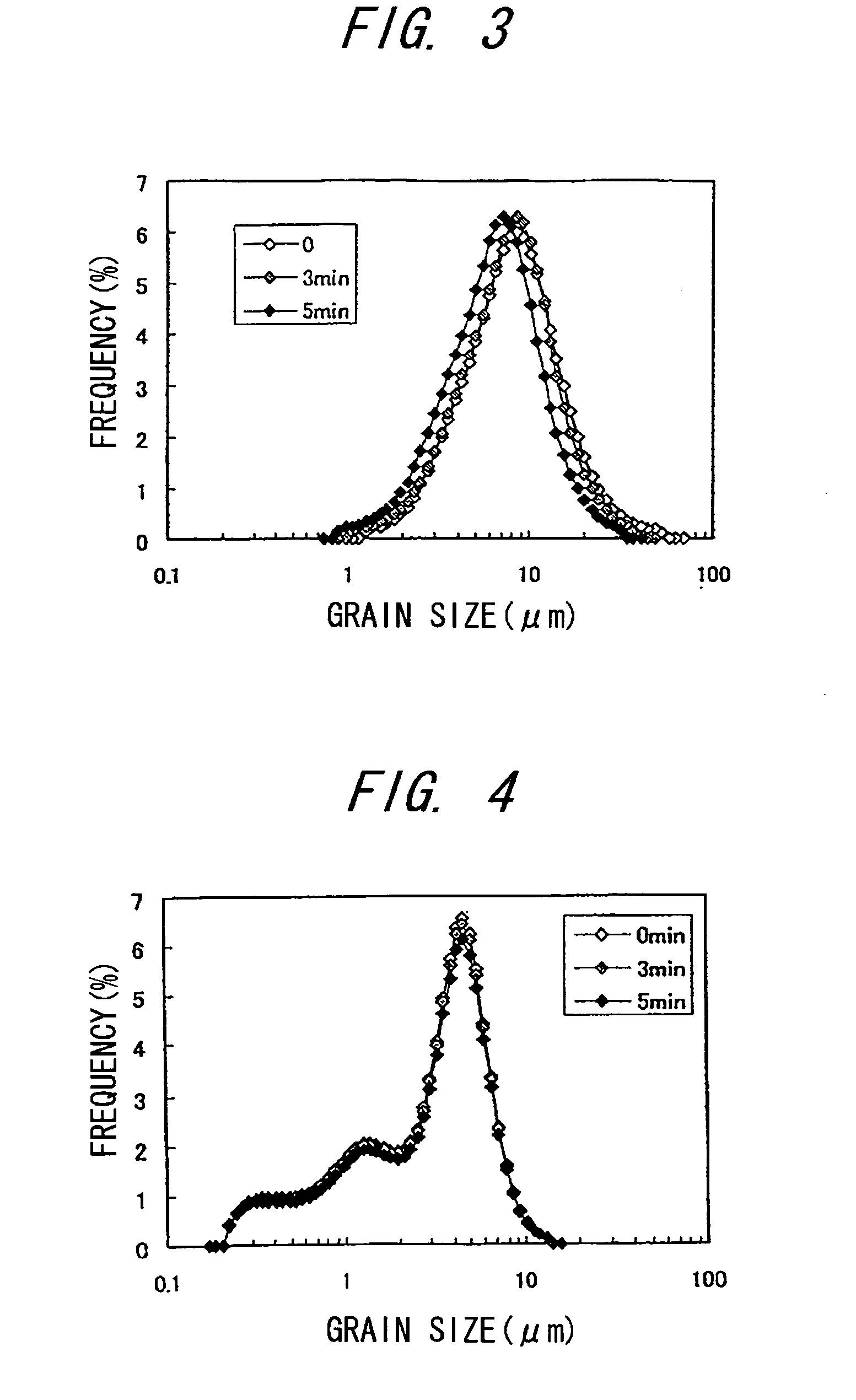
[0088]This Example examined grinding characteristics of an abrasive dissolved and dispersed in pure water, as shown in Table 1, using silica Nos. 1-7 as abrasive grains.

[0089]

TABLE 1CompositionAbrasive content[wt %]ConcentrationSilica (abrasive grains)2011[g / l]Sodium dichloroisocyanurate350.0082[mol / l]Sodium tripolyphosphate220.03[mol / l]Sodium sulfate180.06[mol / l]Sodium carbonate50.025[mol / l]

[0090]First, silica Nos. 1 and 2 use fumed silica with an average grain size of 50 nm measured by the BET method, and aggregated silica grains are formed in the conditions of Table 2. In forming each aggregated silica, fumed silica as an ingredient and a predetermined amount of pure water are mixed uniformly by a Heichel mixer. Subsequently, aggregated silica No. 1 is hot-air dried for 24 hr at 120° C. in a constant-temperature bath, while aggregated silica No. 2 is heat-dried for 2 hr being uniformly mixed at 100° C. by a Heichel mixer. Nos. 1 and 2 are then ground at 25° C. by a pin mill. Aggr...

example 3

[0122]In order to grasp a life of abrasive pads, after an abrasive is prepared using abrasive grains No. 3 of Example 1, an abrasive solution is prepared, and grinding is performed in the same conditions as those of Example 1 (The results are shown in Table 11).

[0123]

TABLE 11WaferSurfaceSilicaGrindingshaperoughness(abrasiveNo. ofspeed(TTV)(Pv)grains)cycles[μm / min][nm][nm]AppearanceNo. 310.60 or more1.43-5Very good450.60 or more0.853-5Very good(peripheraldripping)No. 6460.58 or more1.34-6Very good950.57 or more1.14-6Good

[0124]The result shows that the wafer shape varies little by little from 20 cycles, and at 45 cycles, peripheral dripping in the wafer is remarkable, while the measured value of TTV is 0.85. For this reason, after an abrasive is prepared using abrasive grains No. 6 so that the concentration of sodium tripolyphosphate is 0.05 mol / l in the same manner as Example 2, an abrasive solution is prepared, and grinding is performed in the same conditions as those of Example 1. ...

example 4

[0125]This Example fabricates a semiconductor laser device with MQW (multi-quantum well) structure provided on a GaAs substrate as one example of a semiconductor device. Further, the form of a semiconductor device fabricated with the invention is not limited to the structure of this Example.

[0126]First, using the abrasive solution of Example 1 shown in Table 3, a surface of the (100)-plane GaAs substrate is ground and flatted. The grinding conditions are almost the same as those shown in Table 4: the grinding pressure is 3.5 kPa; the number of revolutions of the plate is about 74 rpm; the abrasive solution supply is 15 ml / min; and the grinding time is about 60 min.

[0127]Subsequently, grinding marks in the surface of the GaAs substrate are removed using a H3PO4:H2O etching solution according to needs. Thereafter, using MBE (molecular beam epitaxy), MOCVD (metal organic chemical vapor deposition), or the like, there are sequentially formed a first GaAlAs cladding layer (film thickness...


PUM

PropertyMeasurementUnit
grain sizeaaaaaaaaaa

Abstract

Abrasive grains have mainly grains with a roundness of 0.50 or more and 0.75 or less, where the roundness is defined as the ratio of the circumference of a circle having the same area as that of a grain to the perimeter of that grain. An abrasive has the abrasive grains and at least one of an oxidizer, an oxide solution, an abrasive grain dispersion agent and a basic compound. An abrasive solution has the abrasive grains and water or hydrophilic substance.

Description

[0001]The present application is based on Japanese patent application No. 2004-080756, the entire contents of which are incorporated herein by reference.BACKGROUND OF THE INVENTION[0002]1. Field of the Invention[0003]This invention relates to grinding abrasive grains suitable for grinding semiconductor wafers such as compound semiconductor wafers (e.g., GaAs wafers), silicon wafers, etc., an abrasive containing the abrasive grains, an abrasive solution containing the abrasive grains, a method for preparing the abrasive solution, a grinding method by the abrasive solution, and a semiconductor device fabrication method using the abrasive solution.[0004]2. Description of the Related Art[0005]In recent years, the flatness of compound semiconductor wafers or semiconductor wafers has been strictly required with remarkable high integration and high capacity, so that still more excellent-precision machining technology has been required. In the grinding step of a wafer fabrication process, t...

Claims


Application Information

Patent Timeline
Patent Type & Authority Patents(United States)
IPC IPC(8): B24D17/00B24B37/00B24D99/00B44C1/22C09K3/14C09K13/00H01L21/302H01L21/304H01L21/306
CPCB24B37/044C09K3/1409C09K3/1463H01L21/02013H01L21/30625
Inventor YOSHIZAWA, CHIEUEMATSU, SATOSHIMASHIYAMA, HISASHITANI, TAKEHIKO
Owner SUMITOMO CHEM CO LTD
Why Eureka
Try Eureka