Surface plasmon enhanced illumination system

a surface plasmon and illumination system technology, applied in the direction of positive displacement liquid engine, microscope, optical radiation measurement, etc., can solve the problems of multi-photon excitation, high cost of clinical use, and inability to resolve distances less than the rayleigh limit, so as to reduce the size of the illuminated area and improve the resolution

Inactive Publication Date: 2008-01-15
PRESIDENT & FELLOWS OF HARVARD COLLEGE
View PDF4 Cites 42 Cited by
  • Summary
  • Abstract
  • Description
  • Claims
  • Application Information

AI Technical Summary

Benefits of technology

[0017]The present invention contemplates a different technique to achieve sub-Rayleigh criterion resolution, which is here called “Surface Plasmon Enhanced Illumination” (SPEI). SPEI is related to NSOM in that nanometric light sources are created by subwavelength apertures. By applying the principles of the present invention, a significant reduction in the size of the area illuminated by each aperture is achieved, resulting in significantly improved resolution.
[0021]Alternatively, the conductive plane that receives the incident light may take the form of a “good metal” layer with a “bad metal” layer having significantly different dielectric properties being sandwiched between the good metal layer and a dielectric substrate. The bad metal layer is preferably opaque to the light to be emitted from the surface of the good metal and its resonance (as determined by its dielectric function, the surface roughness and the dielectric functions of the materials on either side of the bad metal layer) should be very different from the resonance of the “good” metal, such that at desired frequency, light transmitted is emitted only from the holes and not from the exit surface of the array. The insulating dielectric substrate ensures that there can be no surface plasmon excitation from the good metal layer through the light barrier. When a bad metal layer is used that is both opaque to light and has sufficiently different dielectric properties relative to the good metal to eliminate resonant coupling, the dielectric insulator may be eliminated.
[0022]The present invention substantially reduces, compared to an array of subwavelength apertures in a monometallic film such as those described by Ebbesen et al., the size of the area of illumination produced by each aperture using the combination of a metallic layer on which surface plasmons are induced by incident light and surface composed of a material of substantially different dielectric function, such as an insulator or a different metal, so that the excitation of the surface plasmons in the light emitting surface in the exit surface layer will be different than those excited in the metallic layer that is excited by the incident light, and only the light from the decaying resonant surface plasmons of the exit layer will emit from that surface. The photons associated with the resonance of the incident or upper surface will be constrained to exit from the hole itself or from the walls of the hole.
[0024]The invention may advantageously take the form of an array of apertures (holes or slits) formed in structure consisting of a dielectric substrate coated with a conductive metal film on one or both surfaces, or by a thick metallic film, and which further incorporates means for confining the electronic surface excitation to an area immediately adjacent to the apertures where light exits the structure. The means for confining the electronic surface excitation preferably takes the form of a layer of material having dielectric properties that differ substantially from those of the illuminated metal layer, and may consist of a dielectric insulator, a “bad metal” having different dielectric properties, grooves or surface irregularities at the exit surface, or a combination of these. The structure which confines the electronic surface excitation restricts the size of the spot or line of illumination from each aperture, and the use of an array of apertures, or an array of surface irregularities on the metal film, increases the intensity of the illumination from each aperture
[0026]The well defined and highly concentrated areas of illumination created by using such a structure as a light source provide significant advantages in microscopy and in optical data storage devices. The confined illumination patterns produced in accordance with the invention may be used to construct a “Surface Plasmon Enhanced Microscope” (SPEM) exhibiting markedly improved resolution, to construct an optical data storage device capable of storing larger amounts of data in optical storage media with much higher data access rates than is achievable with current optical data storage devices, and to provide a high throughput photolithography technique that can be applied to advantage in semiconductor fabrication and patterning for self-assembly and biological applications.

Problems solved by technology

Typical optical microscopy, far-field light microscopy, cannot resolve distances less than the Rayleigh limit.
This, in turn, not only can cause photo-bleaching in the fluorophores at which one intends to look but also the surrounding area where the light is incident, just not collected.
Multi-photon excitation requires highly skilled technicians and is somewhat expensive for clinical use.
The problem with this technique in determining relative locations is that one of the pair needs to be located within the resolution tolerances desired for spatial mapping.
Another problem is that dipole-dipole interactions are dependent on the relative orientation of the two.
Because only surface morphology is measured, differentiating several molecules can be extremely difficult unless the dimensions and orientations of those molecules are well known.
An associated problem with the “apertureless probes” is that the probe generates a white light continuum, which significantly decreases the signal to noise ratio.
For this reason, NSOM is particularly susceptible to vibrations and experimental work requires isolation platforms.
Scanning the surface takes a fair amount of time.
This can be severely limiting if scanning time is more than a few tens of seconds and resolution less than 50 nm is desired.
If the surface is scanned for several different types of molecules, the required time to investigate a single cell becomes far too large for use in a clinical setting and would require multiple homings of the scanning stage.
This approach would be limited to just a few probes as on a small (202 μm2) surface, the relatively large size of the probes' bodies would interfere mechanically with each other.
Due to the required precision in the location of the four images around the origin and the drift associated with the scanning stage, it is unlikely that the resolution will be dramatically increased.
This, however, can result in severe photo stress to the sample and, possibly, dual photon effects, causing competing modes in the area where quenching is desired.
Once again, though, STED microscopy is a scanning type and will suffer from the same drawbacks all scanning instruments do, (e.g., thermal drift, vibration problems, registration of near field excitement with far field collection and scan time.)

Method used


Image

  • Surface plasmon enhanced illumination system
  • Surface plasmon enhanced illumination system
  • Surface plasmon enhanced illumination system

Examples


Embodiment Construction

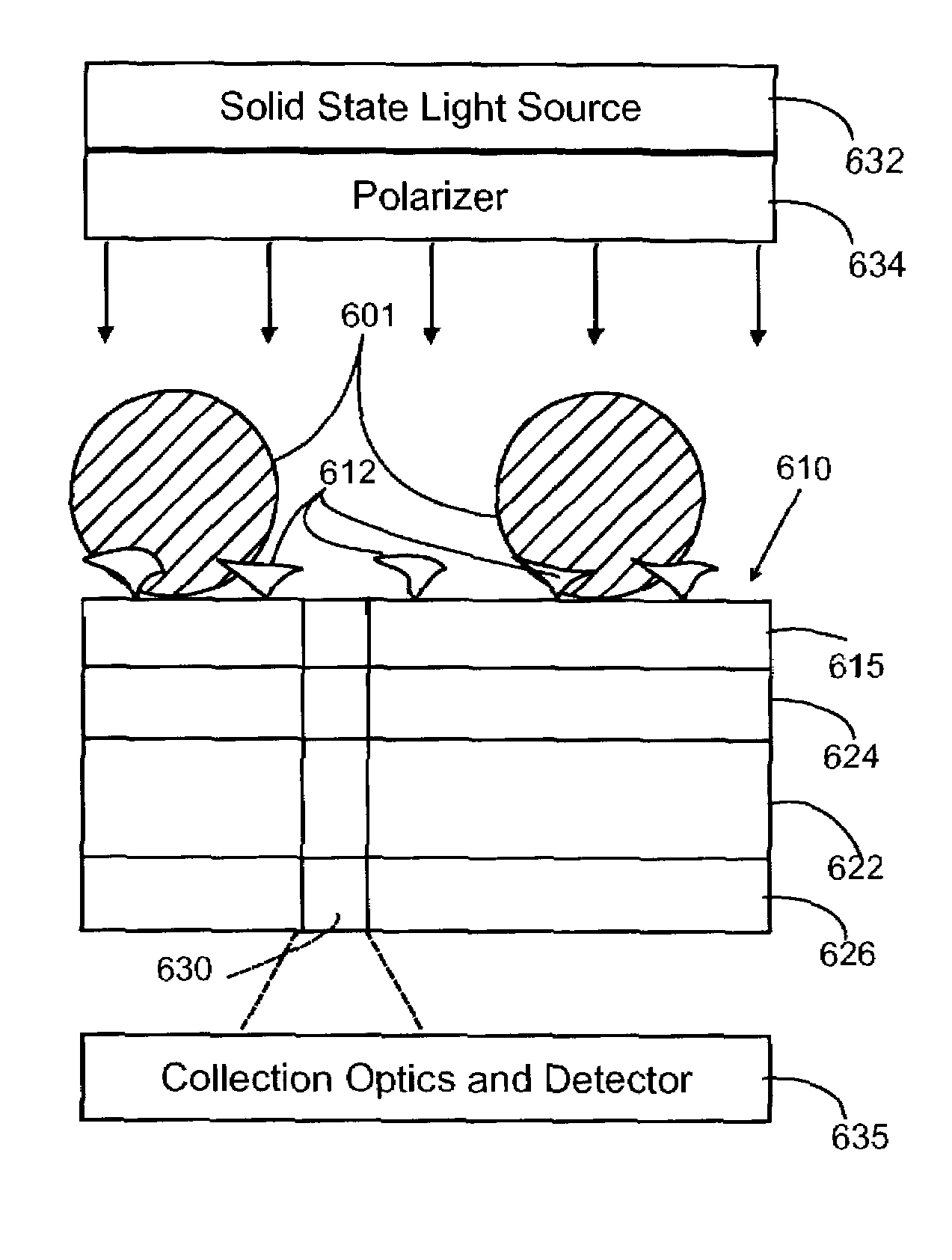
[0061]As described in U.S. Pat. Nos. 5,973,316 and 6,052,238 issued to Ebbesen et al., enhanced light transmission occurs through an array of apertures in a metal film due to the surface plasmons induced in the conductive film by the incident light.

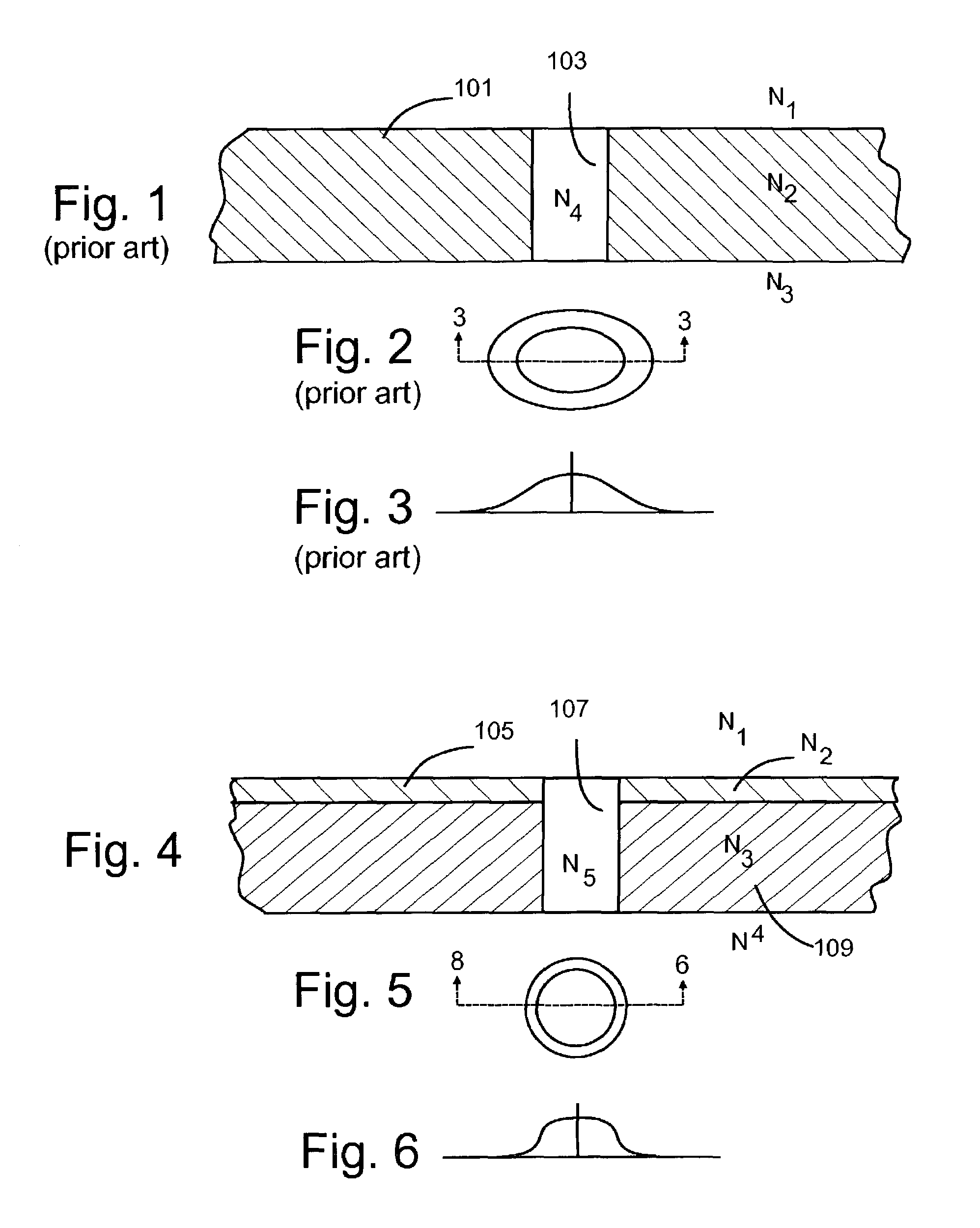
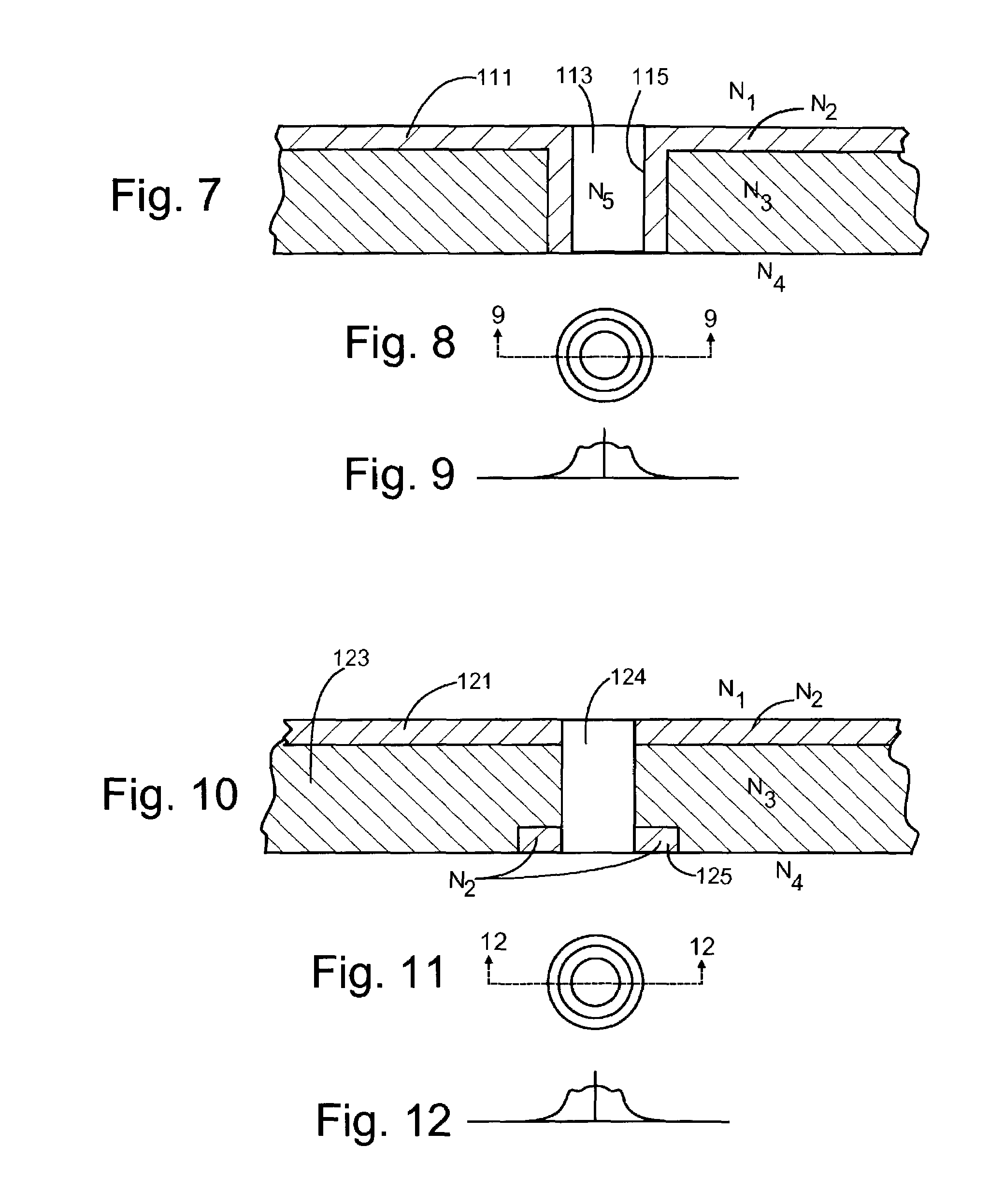
[0062]FIG. 1 shows a cross section of an optically thick metal film 101. The term “optically thick” means that the thickness of the film 101 is greater than two times the skin depth. For all essential purposes, this means that there is no direct coupling of the surface plasmons (coherent collective excitations of electrons) at the upper surface (the interface between media of index N1 and N2) and the lower surface (the interface between media of index N3 and N2). In a typical case, the indices N1, N3, and N4 are equal while N2, the index of the metal film 101, is substantially different and the metal film 101, unlike the surrounding material, is a conductor of electronic charges.

[0063]If the array spacing and the dielectric functions and ...


PUM

PropertyMeasurementUnit
widthaaaaaaaaaa
wavelengthaaaaaaaaaa
Forster distanceaaaaaaaaaa

Abstract

Methods and apparatus for producing small, bright nanometric light sources from apertures that are smaller than the wavelength of the emitted light. Light is directed at a surface layer of metal onto a light barrier structure that includes one or more apertures each of which directs a small spot of light onto a target. The incident light excites surface plasmons (electron density fluctuations) in the top metal surface layer and this energy couples through the apertures to the opposing surface where it is emitted as light from the apertures or from the rims of the apertures. Means are employed to prevent or severely limit the extent to which surface plasmons are induced on the surface at the aperture exit, thereby constraining the resulting emissions to small target areas. The resulting small spot illumination may be used to increase the resolution of microscopes and photolithographic processes, increase the storage capacity and performance of optical data storage systems, and analyze the properties of small objects such as protein and nucleic acid molecules and single cells.

Description

CROSS REFERENCE TO RELATED APPLICATIONS[0001]This application claims the benefit, under 35 U.S.C. §119(e), of the filing date of U.S. Provisional Application Ser. No. 60 / 312,214 filed on Aug. 14, 2001.FIELD OF THE INVENTION[0002]This invention relates to methods and apparatus in which target areas are illuminated with one or more spots or lines of light having very small dimensions and the use of these spots or lines of light and changes to them as a sensing technique.BACKGROUND OF THE INVENTION[0003]Typical optical microscopy, far-field light microscopy, cannot resolve distances less than the Rayleigh limit. The Rayleigh criterion states that two images are regarded as just resolved when the principal maximum (of the Fraunhofer diffraction pattern) of one coincides with the first minimum of the other [see Born, M. and Wolf, E. Principles of Optics. Cambridge University Press 6th ed. p.415 (1980)]. For a circular aperture, this occurs at[0004]w=0.61⁢λNAFor example, the wavelength (λ...

Claims


Application Information

Patent Timeline
Patent Type & Authority Patents(United States)
IPC IPC(8): C12Q1/68G01N15/06G01N33/00G01N33/48G01N35/00A61K31/428G01N21/55G01Q10/00G01Q30/20G01Q60/18G02B21/00G03F7/20G21K1/00G21K5/04H05H6/00
CPCA61K31/428B82Y35/00G01N21/554G01N21/648G02B21/004G02B21/0068G02B21/0072G02B21/0076G03F7/70375G03F7/70483G21K1/00G21K5/04H05H6/00G01Q60/22B82Y20/00Y10T29/49002B82Y30/00H01J2237/3174Y10T29/49Y10T436/11
Inventor STARK, PETER RANDOLPH HAZARDLARSON, DALE N.
Owner PRESIDENT & FELLOWS OF HARVARD COLLEGE
Why Eureka
Try Eureka