Solar cell and its manufacturing method

a solar cell and manufacturing method technology, applied in the field of solar cells, can solve the problems of increasing the amount of abrasive grains retained in the working site, increasing the thickness of the semiconductor single crystal substrate, increasing the cutting width, etc., and achieves the reduction of contact area, energy conversion efficiency, and resistance loss and shadowing loss of the solar cell.

Active Publication Date: 2008-04-08
SHIN ETSU CHEM CO LTD
View PDF9 Cites 47 Cited by
  • Summary
  • Abstract
  • Description
  • Claims
  • Application Information

AI Technical Summary

Benefits of technology

[0012]The inventors found after our extensive investigations that nonconformities such as formation of the electrode on the bottom surface of the grooves and insufficient formation area of the electrodes were effectively avoidable if the minimum depth h of the groove, width W1 of the groove, and angle θ satisfy the condition expressed by the formula (1). Thus-configured solar cell ensures a sufficient depth of groove even for a short groove formed in the thinnest position of a substrate having non-uniform thickness, has the electrodes correctly formed with respect to the thickness-wise direction, and has resistance loss which never exceeds a desired value. The solar cell is also excellent in effect of reducing the shadowing loss, which is an intrinsic object of the OECO solar cells.
[0026]The above-described method of fabricating a solar cell is successful in making the depth of the resultant grooves uniform, and in fabricating a solar cell having a distribution range of groove depth (difference between a maximum value and a minimum value) over the entire surface of the groove-forming surface suppressed to as small as ±5% or less of a distribution range of substrate thickness (difference between a maximum thickness and a minimum thickness).

Problems solved by technology

The slicing using the wire saw is, however, disadvantageous in that the amount of an abrasive grain retained in the working site increases as the depth of cutting into the ingot increases, and this gradually increases the cutting width.
It is thus understood that use of the as-sliced semiconductor single crystal substrate 24′ is advantageous in reducing the production costs to a considerable degree through shortening of the process time, but is disadvantageous in making the thickness of the semiconductor single crystal substrate 24′ non-uniform.
Any conventional method of carving the grooves on the substrate 24′ for fabricating the solar cells will be unsuccessful in obtaining a constant depth of the grooves 2′ as measured from the light-receiving surface 1′a over the entire surface because of the non-uniformity in the thickness of the substrate 24′.
On the substrate 24′ having the grooves of non-uniform depths, formation of the electrodes 6′ on the side faces 2′a of the grooves by the above-described vapor deposition process will result in heights of the electrode 6′ smaller than the designed values, or undesirable deposition of the metal also on the bottom surface 2′c of the grooves.
The formation of the metal on the bottom surface 2′c of the groove will increase the shadowing loss and thus ruin the energy conversion efficiency.
Etching for removing the excessive deposition of the metal will, however, decrease electrode forming area and will thus increase the resistance loss.
Both increases in the shadowing loss and resistance loss result in lowering of the energy conversion efficiency of the solar cell as a natural consequence.
In an exemplary case where the depth of the groove for electrode contact carved on the back surface of the solar cell is larger than a designed value, the boundary area between the electrode and substrate increases, and this results in increase in recombination rate at the boundary.
On the contrary, the depth smaller than the designed value result in poor contact between the electrode and substrate, and this increases the contact resistance.
These variations in the characteristics result in variation in the output voltage, and may eventually lower the output of the solar cell.

Method used


Image

  • Solar cell and its manufacturing method
  • Solar cell and its manufacturing method
  • Solar cell and its manufacturing method

Examples


first embodiment 1

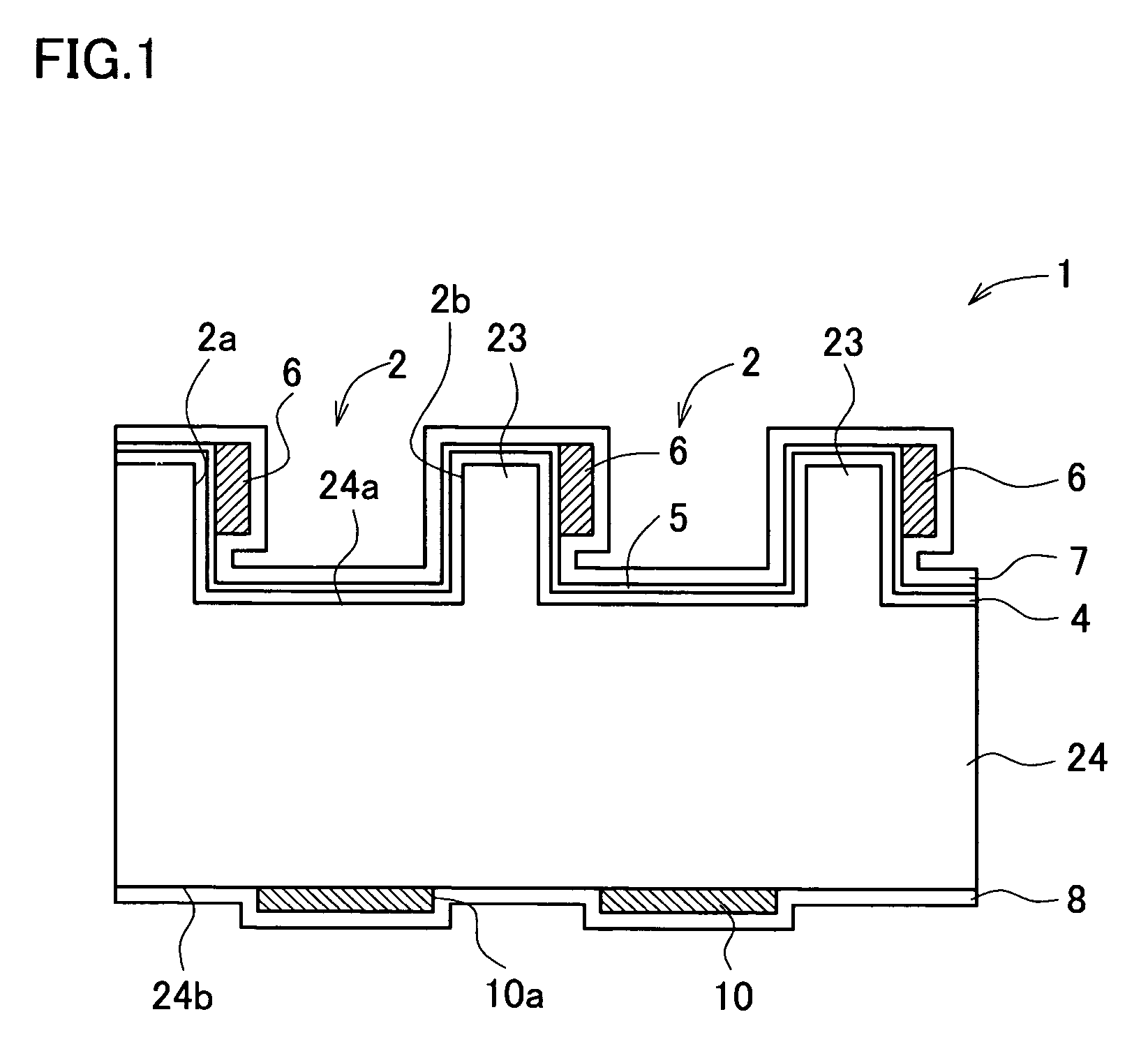
[0055]FIG. 1 is an enlarged sectional view partially showing one embodiment of a solar cell according to a first aspect of the invention. The solar cell 1 is configured so that a large number of grooves 2 of several-hundred-micrometers wide and approximately several tens micrometers to 100 μm deep are formed in parallel on the first main surface 24a of a p-type silicon single crystal substrate 24 sliced out from a silicon single crystal ingot. These grooves 2 can be carved en bloc using a set of hundreds to thousands of concentrically-joined rotary cutting edges which rotate all together, where it is also allowable to divide the carving operation into several numbers of run.

[0056]On the first main surface 24a of the substrate 24 having the grooves 2 thus formed thereon, an emitter layer 4 is formed by thermally diffusing phosphorus as an n-type dopant, so as to produce a p-n junction portion. On the emitter layer 4, a thin silicon oxide film 5 which functions as a tunnel insulating ...

second embodiment

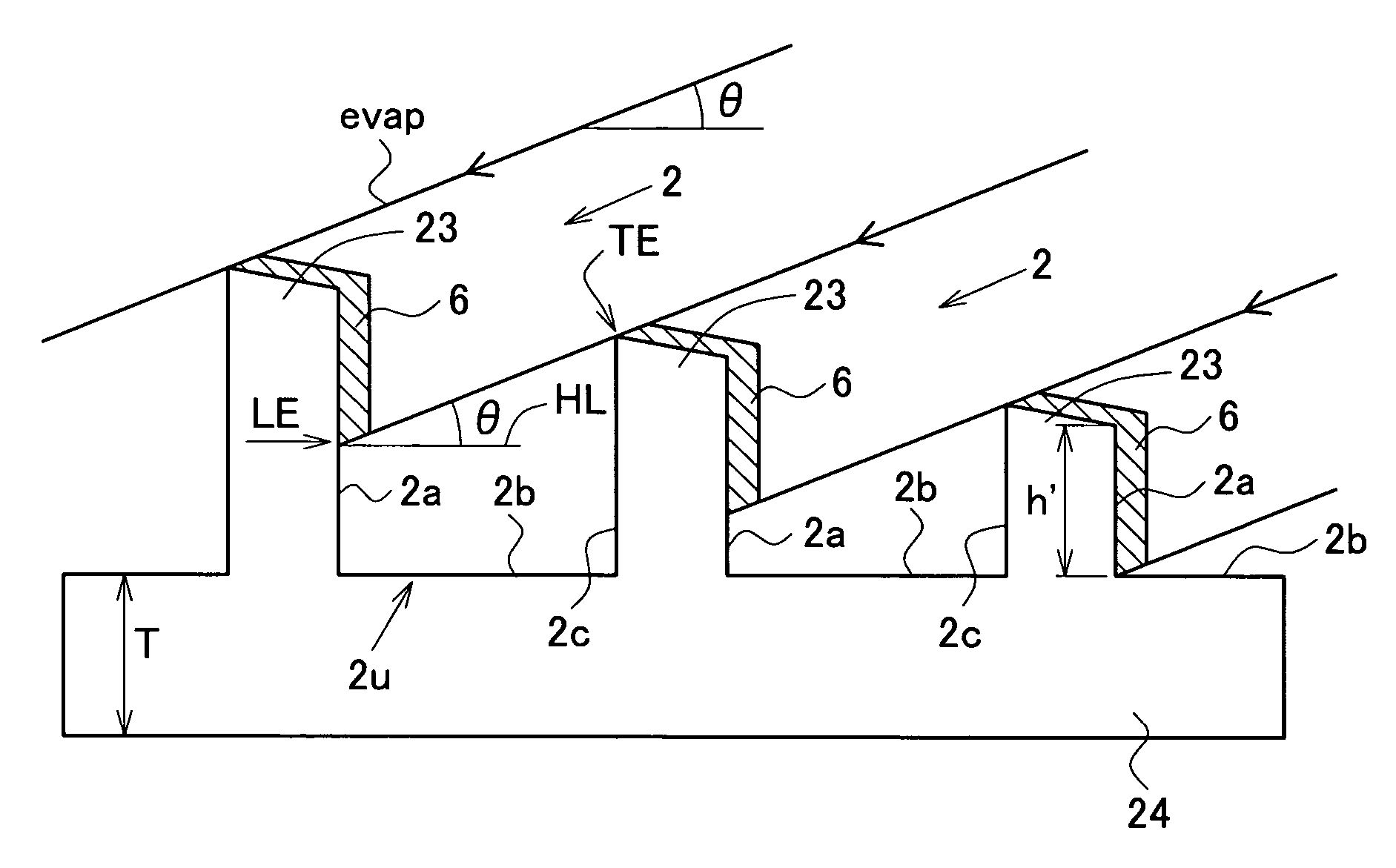
[0084]An embodiment of the method of fabricating the solar cell according to the second aspect of the invention will be described. A target solar cell in the second embodiment is again the OECO cell shown in FIG. 1, similarly to the first embodiment. The aforementioned first embodiment used the upward-edge-type, high-speed rotary blade, dared to allow variation in the depth of the grooves 2 to generate according to the non-uniformity in the substrate thickness, and instead imposed the limitation expressed by the formula (1) on the depth of groove h′ at the thinnest position in order to reduce the shadowing loss and electrode resistance loss. On the contrary, the present second aspect aims at equalizing the groove depths within a single substrate as possible.

[0085]In the present embodiment, a p-type silicon single crystal ingot, which is prepared by adding a Group Ill element such as boron or gallium to a high-purity silicon and manufactured by the CZ method or FZ method, is obtained...

example 1

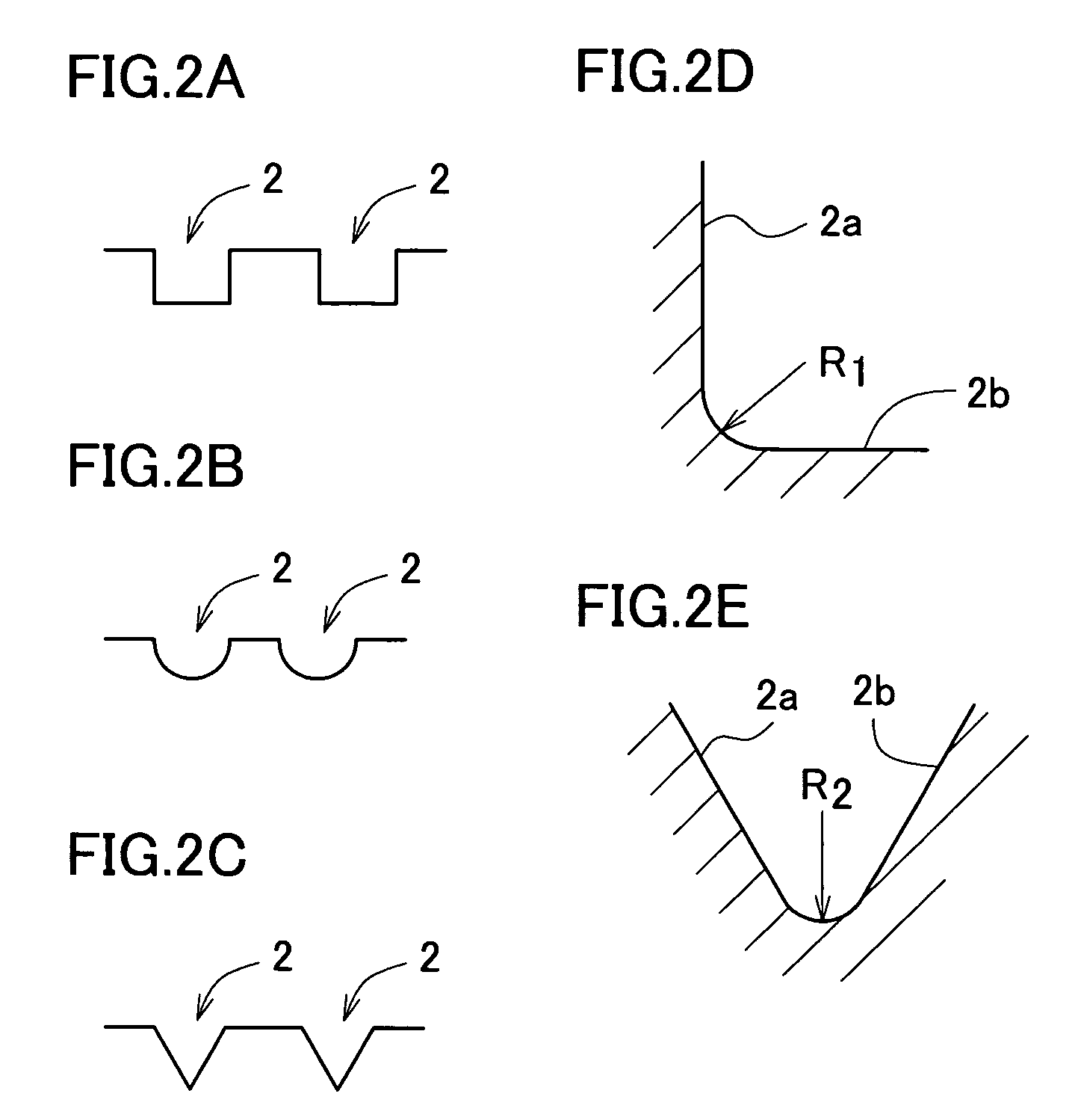
[0094]A p-type single crystal silicon wafer 1 for fabricating solar cells, containing gallium, which is a Group III element, as an impurity element (diameter=4 inches, minimum thickness=270 μm, maximum thickness=300 μm, resistivity=0.5 Ω·cm) was obtained, and the thickness distribution thereof was preliminarily measured using a dial gouge. Based on the measured results, a plurality of parallel grooves 2 having a rectangular section were formed as shown in FIG. 3 using a dicing saw (high-speed rotary blade) in parallel to a line connecting the thickest position and thinnest position of the wafer. The edge portion of the grinding blade used herein was 450 μm in thickness, 50 mm in diameter and had an inter-edge interval of 50 μm. Based on the thickness of the grinding blade defined as 450 μm and on the angle of deposition, described later, as 5°, the minimum depth of the groove h was defined as 50 μm. Process conditions defined herein included a speed of rotation of the grinding blade...


PUM


Abstract

An OECO solar cell using a semiconductor single crystal substrate having a plurality of grooves, wherein a minimum groove depth h of each groove always satisfies the relation of h≧W1tan θ where θ represents an angle between a line connecting the lower end, along the thickness-wise direction of the semiconductor single crystal substrate, of an electrode formed in the groove and the upper end of the inner side face of the same groove having no electrode formed thereon, and a reference line normal to the thickness-wise direction, and W1 represents a distance between both opening edges of the groove; wherein the semiconductor single crystal substrate has thickness decreasing from a first side of a first main surface to a second side opposed to the first side; and wherein the plurality of grooves have a depth distribution of being deepest at a thickest position of the substrate, and a gradually becoming shallower towards a thinnest position of the substrate.

Description

TECHNICAL FIELD[0001]This invention relates to a solar cell and a method of fabricating the solar cell.BACKGROUND ART[0002]Recent demands for solar cells are directed to higher efficiency and lower costs at the same time. In this context, the OECO (obliquely evaporated contact) process attracts public spotlight. The OECO process is a method of fabricating solar cells proposed by R. Hezel et al. of Institut für Solarenergieforschung GmbH Hameln / Emmerthal (ISFH), Germany, and is representatively disclosed in Renewable Energy, Vol. 14, p.83 (1998) (a solar cell fabricated by the OECO process may occasionally be referred to as OECO solar cell, hereinafter). A method of fabricating the OECO cell will briefly be explained referring to FIG. 12. The OECO solar cell is configured so that a plurality parallel grooves 2′ (having a sectional form of rectangular, semicircle, triangular or the like) are carved on the main surface, which later serves as a light-receiving surface, of a silicon sing...

Claims


Application Information

Patent Timeline
Patent Type & Authority Patents(United States)
IPC IPC(8): H01L31/0248H01L31/068H01L31/0224H01L31/0236H01L31/0352H01L31/04
CPCH01L31/022433H01L31/02363H01L31/035281H01L31/03529H01L31/068H01L31/1804Y02E10/547Y02P70/50H01L31/04H01L31/18
Inventor OJIMA, SATOYUKIOHTSUKA, HIROYUKITAKAHASHI, MASATOSHIWATABE, TAKENORI
Owner SHIN ETSU CHEM CO LTD
Why Eureka
Try Eureka