
Variable gain amplifier and variable gain amplifier module

a variable gain amplifier and amplifier technology, applied in the field of semiconductor circuit technology, can solve the problems of complex structure and excessive current consumption, and achieve the effect of simple structur

Active Publication Date: 2008-06-24
ELECTRONICS & TELECOMM RES INST
View PDF10 Cites 8 Cited by
  • Summary
  • Abstract
  • Description
  • Claims
  • Application Information

AI Technical Summary

Benefits of technology

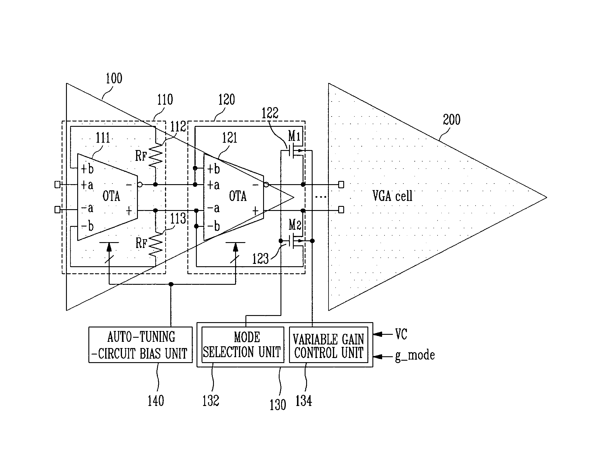
The present invention is about a variable gain amplifier (VGA) that has a simple structure and a linear variable gain characteristic on a logarithmic scale. The invention also proposes a circuit structure that consumes low power and has a small size to be applied to a core chip of a terminal. The invention provides a basic block of a VGA comprising a frequency compensation input unit, a gain amplification unit, and a control unit. The invention also provides a VGA module comprising a first operational transconductance amplifier (OTA), a first variable resistor, a second OTA, a first fixed resistor, a second fixed resistor, and a differential gain amplifier. The invention allows for a broader gain adjustment range and can be used in multiple stages for more precise adjustments. The technical effects of the invention include a simplified structure, a linear variable gain characteristic, low power consumption, and a small size.

Problems solved by technology

However, such CMOS VGAs use many blocks to overcome characteristics of a CMOS device and obtain a linear gain characteristic on a logarithmic scale, which results in a complicated structure and excessive current consumption.

Method used


Image

  • Variable gain amplifier and variable gain amplifier module
  • Variable gain amplifier and variable gain amplifier module
  • Variable gain amplifier and variable gain amplifier module

Examples


Embodiment Construction

[0025]Hereinafter, an exemplary embodiment of the present invention will be described in detail. However, the present invention is not limited to the exemplary embodiments disclosed below, but can be implemented in various types. Therefore, the present embodiment is provided for complete disclosure of the present invention and to fully inform the scope of the present invention to those ordinarily skilled in the art

[0026]In general, an operational transconductance amplifier (OTA) having a characteristic of a voltage-current converter has an input / output characteristic that is linear for a considerably wide range, and thus is used in many circuit blocks. In particular, an analog low-frequency filter used in most terminals is designed using such an OTA. Examples of applications of such an OTA are a biquad type filter or an inductor-capacitor (LC) ladder type filter applying a gyrator. In the OTA, a transconductance Gm is stably and minutely controlled by an auto tuning circuit in a sys...


PUM


Abstract

An analog variable gain amplifier (VGA) adjusting a signal level of a mobile communication system is provided. More particularly, design of a VGA using an operational transconductance amplifier (OTA) having a wide linear input / output range is disclosed. The VGA includes two double-differential-pair OTAs and feedback resistors. A first differential input of a first double differential pair OTA receives an input signal from the forward stage, and a second differential input is negatively fed back through a differential output and a passive resistor. An input in which a first block of the connection structure and first and second differential inputs of a second double differential pair OTA are connected receives an output signal of the first block stage. The output is negatively fed back in series through a variable resistor whose resistance varies exponentially with an adjustment voltage from outside. According to the VGA, it is possible to provide a characteristic of linear variation of gain on a logarithmic scale with respect to a control voltage with a simple and inexpensive constitution. In addition, the VGA can be designed for a low pass filter having a conventional OTA used for a core circuit, and has a simple circuit structure. Therefore, the VGA is convenient for high integration and low-power design, and thus is appropriate for a terminal chip and so forth.

Description

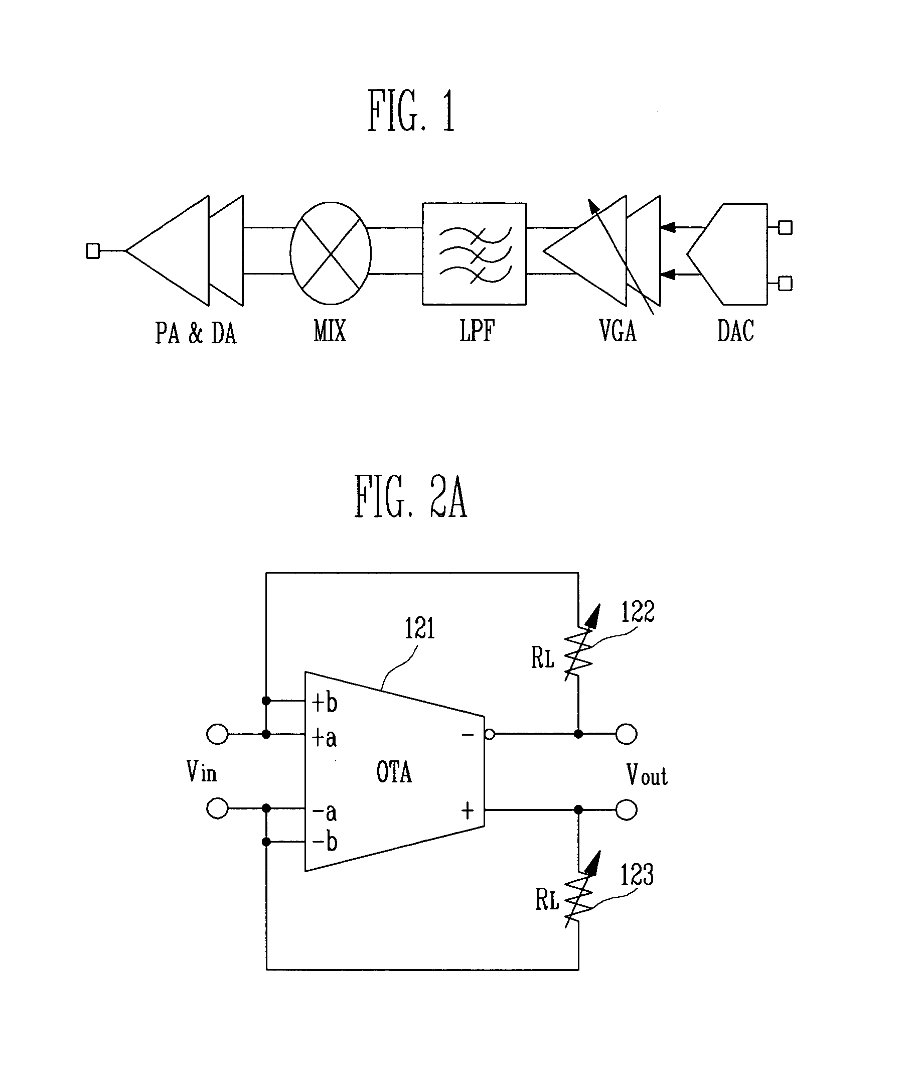
CROSS-REFERENCE TO RELATED APPLICATION[0001]This application claims priority to and the benefit of Korean Patent Application No. 2005-118073, filed Dec. 6, 2005, the disclosure of which is incorporated herein by reference in its entirety.BACKGROUND[0002]1. Field of the Invention[0003]The present invention relates to semiconductor circuit technology, and more particularly, to an analog variable gain amplifier (VGA) adjusting a signal level of a mobile communication system, and even more particularly, to design of a VGA employing an operational transconductance amplifier (OTA) having a wide linear input / output range.[0004]2. Discussion of Related Art[0005]In a mobile communication terminal illustrated in FIG. 1, transmission power of a transmitter should be controlled in order to avoid excessive interference with another terminal. Such power control is performed by an automatic gain control (AGC) circuit, thereby maximizing a dynamic range of the entire system. The core cell of the AG...

Claims


Application Information

Patent Timeline
Patent Type & Authority Patents(United States)
IPC IPC(8): H03F1/36H03F3/45
CPCH03F1/08H03F1/34H03F3/45475H03G1/007H03F2200/381H03F2203/45138H03F2203/45522H03F2203/45524H03F3/45
Inventor KIM, YOUNG HOPARK, MUN YANGYU, HYUN KYU
Owner ELECTRONICS & TELECOMM RES INST
Learn More