Fabrication method of a semiconductor device using liquid repellent film

a technology of liquid repellent film and semiconductor device, which is applied in the direction of optics, instruments, transistors, etc., can solve the problems of contact defect, and achieve the effects of good contact hole, reduced process complexity, and improved contact hole quality

Inactive Publication Date: 2008-07-15
SEMICON ENERGY LAB CO LTD
View PDF72 Cites 24 Cited by
  • Summary
  • Abstract
  • Description
  • Claims
  • Application Information

AI Technical Summary

Benefits of technology

[0007]The present invention has been made in view of the above problems and it is an object of the present invention to propose a method for forming a good contact hole and insulating films provided over the contact hole, such as an interlayer insulating film, a planarizing film, a gate insulating film, and the like. It is a further object of the present invention to provide a method for fabricating a semiconductor device with high yield and high throughput at low cost.
[0013]Note that, in the case where the first organic film is not intrinsically liquid repellent, the first organic film is treated with plasma, a laser, an electron beam, or the like before forming the second organic film. The surface of the first organic film can be made liquid repellent by the treatment, and the second organic film can be prevented from adhering to the first organic film. Thus, a good contact hole can be made. Naturally, when the first organic film is made of a material that is liquid repellent, such treatment can be omitted, or can be performed in order to improve the liquid repellency.
[0017]As in the invention, a liquid repellent material is used for the first organic film (a film provided at a part to be a contact hole), so that the second organic film serving as an interlayer insulating film, a planarizing film, a gate insulating film, or the like may be formed at the predetermined portion. Besides, the insulating films can be formed in and around the contact hole without performing exposure or development using a resist mask; thus, the process can be significantly simplified as compared with conventional process. Further, the second organic film is not formed on the first organic film, so that the first organic film can be removed more easily and a good contact hole can be formed through a simple process.
[0018]Even in the case of using a material which is not liquid repellent for the first organic film, the first organic film may be made repellent by liquid repellent treatment with plasma, a laser, an electron beam, or the like before forming the second organic film. Thus, wider options of materials can be offered. Further, in the case of using a material which is intrinsically liquid repellent, the repellency can be improved by the treatment.
[0019]In forming the first organic film, a conductive film, and the like, liquid containing the material of the films can be applied to an arbitrary area by changing the relative positions of the substrate and a nozzle from which the liquid is discharged by a droplet discharge method. Further, the thickness or the width of the patterns to be formed can be controlled by the nozzle diameter, the liquid discharge rate, and relative relationship among the movement speeds of the nozzle and the substrate where the discharged material is applied. Thus, the material of the films can be accurately discharged and the films can be formed in the desired area. Since a patterning process, that is exposure and development using a resist mask, can be omitted, significant simplification of the process and the cost reduction can be attempted. Further, by using the droplet discharge method, patterns can be formed on an arbitrary area and the thickness and the width of the patterns to be formed can be controlled. Thus, even a large semiconductor element substrate having a side of 1 m to 2 m can be fabricated with high yield at low cost.
[0020]As described above, a contact hole of a semiconductor device and an insulating film therearound can be formed accurately through a simple process. Further, a method for fabricating a semiconductor device with high throughput and high yield at low cost.

Problems solved by technology

Further, even though the throughput is improved, the resist spreads to the area of a contact hole when the surface state of the base and the amount of the resist to be applied are not fully controlled; thus, the contact defect would occur.

Method used


Image

  • Fabrication method of a semiconductor device using liquid repellent film
  • Fabrication method of a semiconductor device using liquid repellent film
  • Fabrication method of a semiconductor device using liquid repellent film

Examples


embodiment mode 1

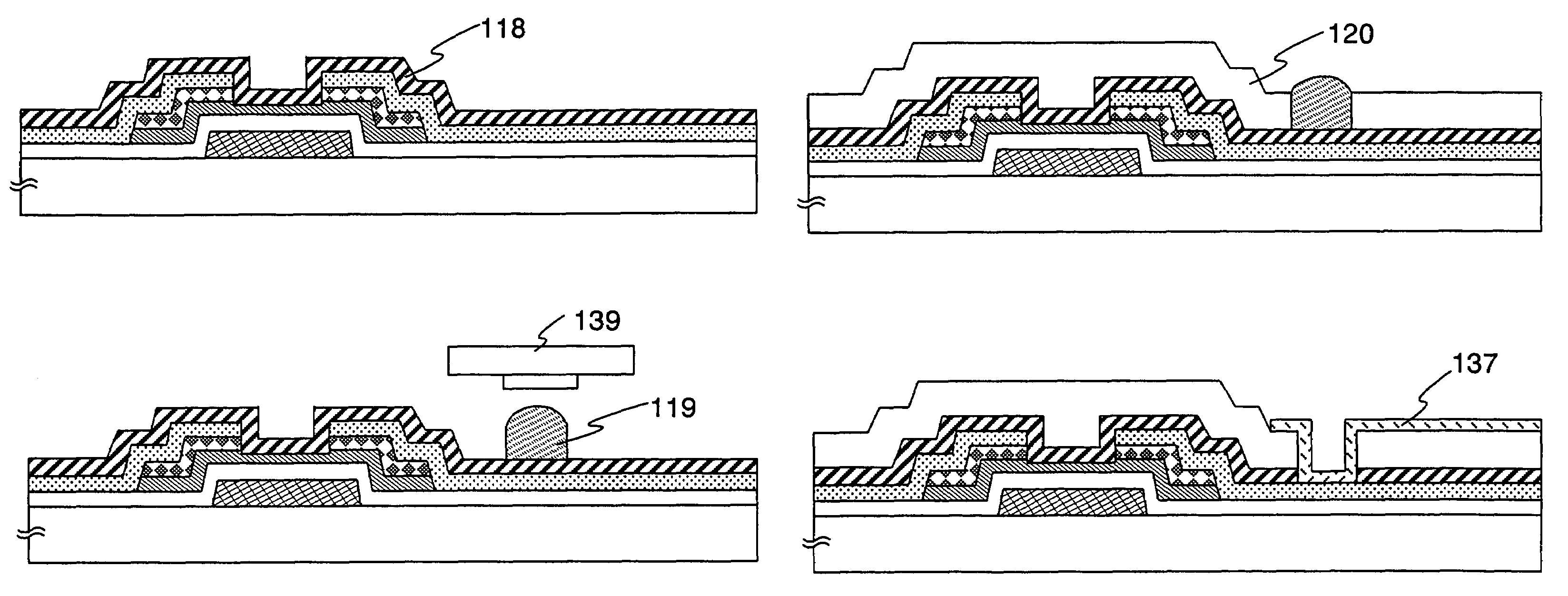
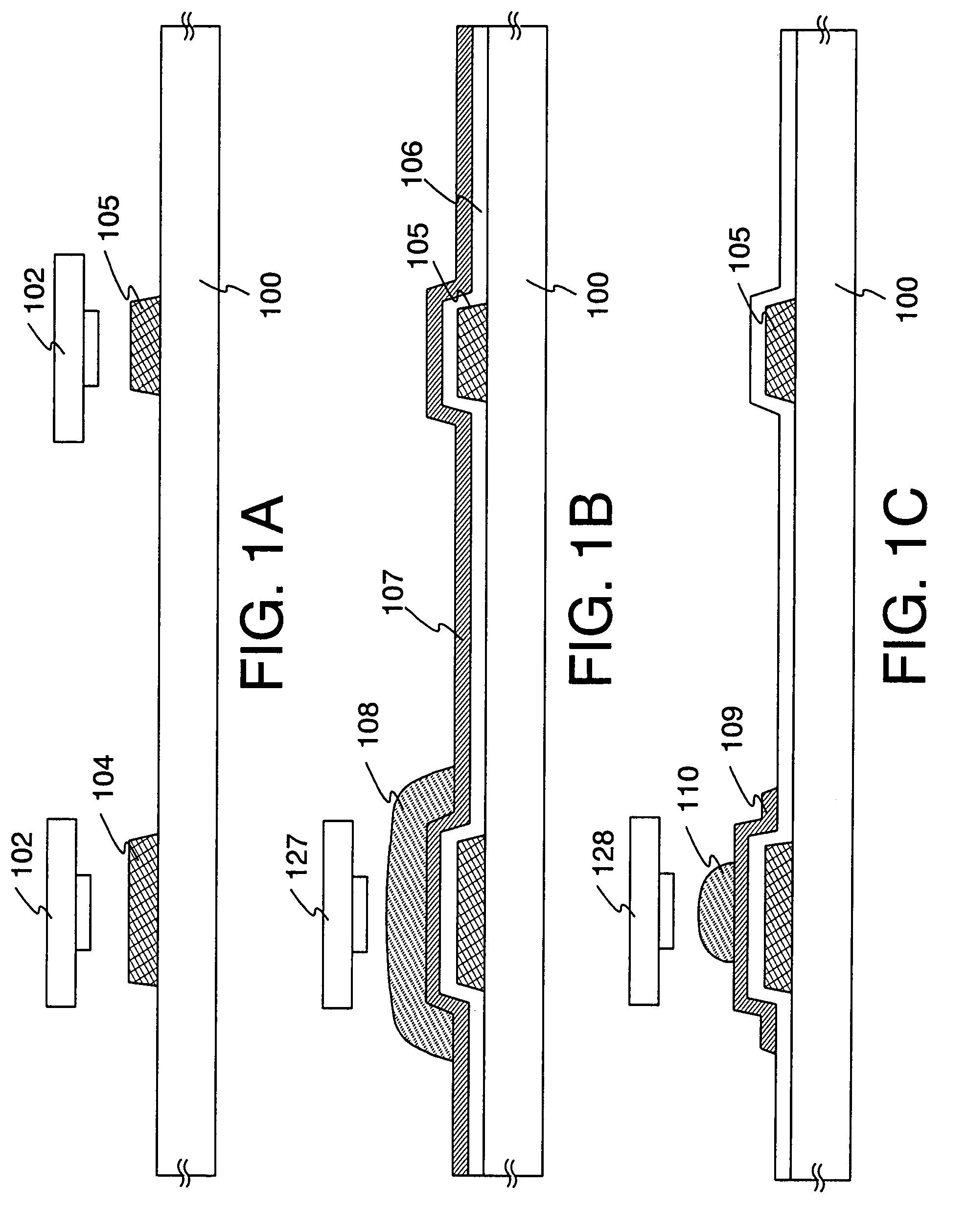
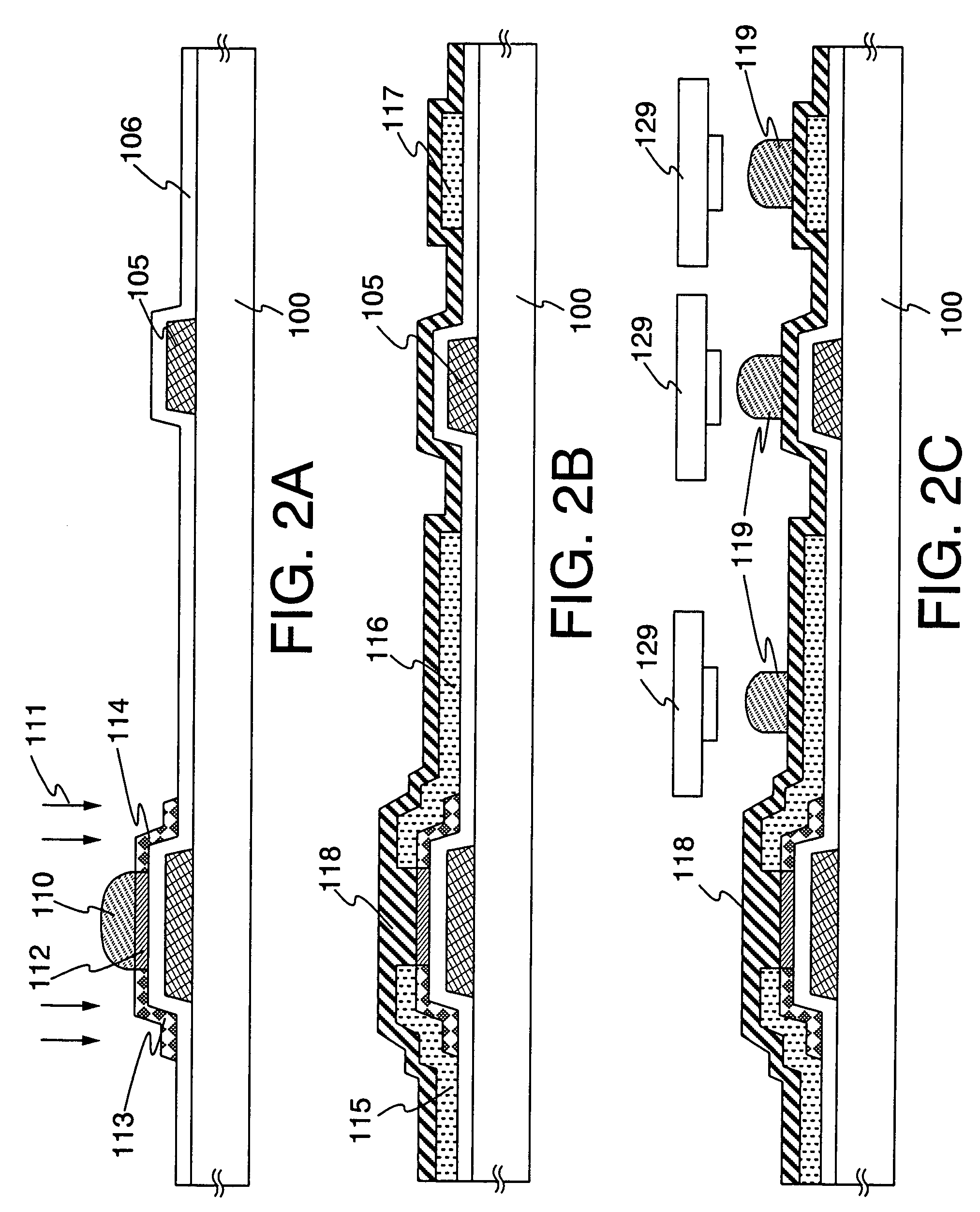
[0040]In this embodiment mode, the case of applying the present invention to the fabrication of an inverted staggered (bottom gate type) TFT will be described with reference to FIGS. 1A to 3C.

[0041]First, a gate electrode 104 and a scan line 105 supplying a signal to the gate electrode 104 is formed over the substrate 100. It is preferable that the gate electrode 104 and the scan line 105 are formed over the substrate 100 by selectively discharging each composition containing a conductive material. In this case, etching using a mask pattern is not required, so that the number of the fabrication process can be significantly simplified.

[0042]The diameter of nozzles 102 used as a liquid discharge means is each set at 0.1 μm to 50 μm (preferably, 0.6 μm to 26 μm), and the discharge amount of the composition discharged from the nozzles 102 is each set at 0.00001 pl to 50 pl (preferably, 0.0001 pl to 10 pl). The discharge amount increases in proportion with the diameters of the nozzles 10...

embodiment mode 2

[0092]In this embodiment mode, the case of applying the invention to the fabrication of a top gate TFT will be described with reference to FIGS. 4A to 5D.

[0093]First, a semiconductor film 401 is formed over the substrate 100 having an insulating surface. The substrate 100 may use a substrate formed of an insulating material such as glass, quartz, or alumina; or metal such as stainless steel or a semiconductor substrate whose surface is provided with an insulating film of such as silicon oxide, silicon nitride, or the like. Alternatively, a flexible or nonflexible plastic substrate which is heat resistant so as to endure the highest processing temperature in this process such as a baking temperature of the pattern formed by a droplet discharge method, or a heat treatment temperature of activation of impurities doped into a source and a drain regions of the semiconductor device.

[0094]The semiconductor film 401 is formed of an amorphous semiconductor, a crystalline semiconductor, or a ...

embodiment 1

[0116]In this embodiment, the fabrication method of an active matrix substrate with the use of the invention will be described with reference to FIG. 6A to FIG. 8B. In particular, the case of using PVA for first organic films and using polyimide or acrylic for a second organic film in order to form contact holes will be described.

[0117]First, a base insulating film 601 is formed over a substrate 600. Here, a silicon oxynitride film (SiNO) is formed to a thickness of 10 nm to 200 nm by plasma CVD to form the base insulating film 601. The material of the base insulating film 601 is not limited to SiNO, and a silicon film oxide, a silicon nitride film, or a silicon oxynitride film; or a stack thereof may be used. Further, the base insulating film 601 is not necessarily formed.

[0118]Next, a semiconductor film is formed to a thickness of 10 nm to 80 nm over the base insulating film 601. The surface of the semiconductor film is treated with a solution containing nickel, and a crystalline ...


PUM

PropertyMeasurementUnit
diameteraaaaaaaaaa
diameteraaaaaaaaaa
distanceaaaaaaaaaa

Abstract

In the case where a contact hole is formed by a conventional process of the semiconductor device fabrication, a resist is required to be formed almost entirely over a substrate in order to form the resist over the film where the contact hole is not formed. Accordingly, the throughput is considerably low. Further, when the resist spreads to the area of the contact hole when the amount of the resist to be applied and the surface state of the base are not fully controlled, contact defect would occur. Thus, improvements are required. According to the invention, in forming a semiconductor device, a part to be a contact hole of the semiconductor device may be covered with a first organic film that is liquid repellent. Subsequently, a second organic film serving as an insulating film is formed on the area where the first organic film is not formed, and the first organic film is removed thereafter to form a contact hole.

Description

BACKGROUND OF THE INVENTION[0001]1. Field of the Invention[0002]The invention relates to a fabrication method of a semiconductor device using a droplet discharge method typified by ink-jet method. The invention particularly relates to a technology for forming a contact hole provided in a semiconductor device.[0003]2. Description of the Related Art[0004]With respect to the fabrication of a semiconductor device, the use of a droplet discharge system is considered to form a thin film or a pattern of a wiring in view of the cost reduction of facilities and simplification of the process.[0005]The following method has been taken in forming a contact hole in a semiconductor device. First, photolithography is performed as a resist is applied entirely over a substrate and prebaked; ultraviolet radiation is applied through a mask; and the substrate is exposed thereafter to form a resist pattern. Subsequently, parts of an insulating film, a semiconductor film, a conductive film, and the like, ...

Claims


Application Information

Patent Timeline
Patent Type & Authority Patents(United States)
IPC IPC(8): H01L21/44H01L21/28G02F1/136G02F1/1368G03F7/004H01L21/00H01L21/027H01L21/311H01L21/312H01L21/336H01L21/461H01L21/4763H01L21/768H01L21/77H01L21/84H01L27/02H01L27/12H01L29/786H01L51/00H01L51/40
CPCG02F1/1368H01L21/31138H01L21/31144H01L21/3121H01L21/76802H01L27/1292H01L29/66757H01L29/66765H01L27/1248H01L27/12H01L51/0016H01L21/02118H01L21/0212H01L21/02126H10K71/221H01L21/28H01L21/0234
Inventor FUJII, GENMAEKAWA, SHINJI
Owner SEMICON ENERGY LAB CO LTD
Why Eureka
Try Eureka