
Array of parallel programmable processing engines and deterministic method of operating the same

Inactive Publication Date: 2008-07-15
TRANSWITCH
View PDF8 Cites 89 Cited by
  • Summary
  • Abstract
  • Description
  • Claims
  • Application Information

AI Technical Summary

Benefits of technology

[0049]Each PE preferably has multi-threading capabilities, which makes an efficient implementation of multi-threading descriptions possible. Moreover, the architecture of each PE can preferably tuned for application specific extensions, which makes it possible to exploit the fine-grain parallelism (if necessary) by adding functional units that implement dedicated instructions (e.g. cyclic redundancy checks). The functional units may be themselves programmable. For instance they may be formed of digital programmable logic elements such as PALs (Programmable Array Logic), PLAs (Programmable Logic Array), PGAs (Programmable Gate Array) and in particular FPGAs (Field Programmable Gate Array). The switching network may employ various types of routing, e.g. wormhole routing and can achieve a communication bandwidth very close to a network of dedicated busses, without the drawbacks of a multiple bus network.
[0055]The CPPA architecture of the present invention has many advantages:
[0056]It is programmable. Therefore, it offers flexibility to deal with errors and changing requirements, without expensive re-spins.
[0063]With progress of VLSI technology and the use of small RISC architectures many nodes in accordance with the present invention can be integrated in a single chip. This creates the potential for extremely efficient inter-node communication, using the network techniques described in the present invention.

Problems solved by technology

However, due to the limitations of the designer and design tools, there is a limit to the content of the specification for which the semantic gap can be bridged at reasonable cost.
Consequently, if the semantics of the design language remain constant, then progress in VLSI technology will inevitably lead to a design crisis.
At present, IC designers are again confronted with a design crisis.
The state-of-the-art design methodology is rapidly becoming inadequate to handle the design challenges of Systems-On-Chip (SoC) products.
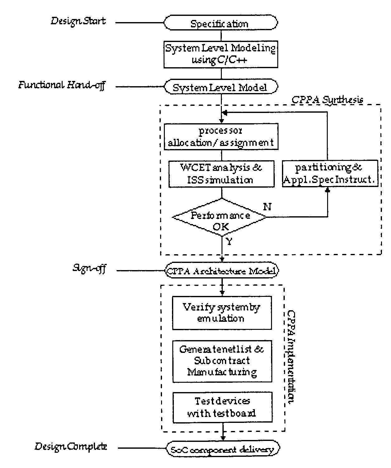
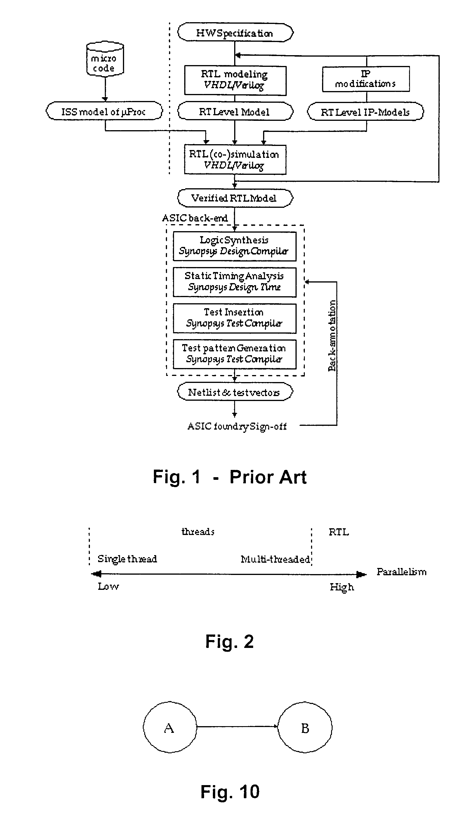
The shortcomings of the current design flow are the following:The design productivity of an RTL based design flow incurs unacceptable design cost and time-to-market.
Even if it is assumed that the design productivity is 1000 gates / person-day (which is very competitive), the design would require 8000 person-days or more than 36 man-years.Simulations at the RT level are too slow for adequate, pre-manufacturing verification.
The number of cycles that can be simulated per second (the simulation speed) decreases because the system complexity increases the amount of computations per cycle.
In addition, the number of cycles that must be simulated for sufficient verification coverage also increases because of the increased system complexity.
These two factors make it virtually impossible to achieve first-time-right designs with an RTL based approach to SoC design, leading to expensive and time consuming device re-spins.To boost the design productivity, previously designed units need to be reused.
However, reuse of design units is seldom possible as is.
However, the RTL-based design flow does not address this issue.
Both levels are too low to enable the simulation speed required for sufficient verification coverage.Logic synthesis performs netlist optimisations based on area and performance estimates of design options.
However, with deep sub-micron technologies, these estimates are becoming less accurate because the actual performance depends to a large extent on the detailed placement and routing, which is not yet available during synthesis.
A large number of synthesis / placement & routing iterations may result before an implementation is found that matches the performance requirements.
A design crisis as mentioned above is often attributed to the growing gap between design complexity and design productivity.
This is, however, an oversimplification of the problem.
The gap between design complexity and design productivity is not the cause of the design crisis, but merely a symptom of the semantic gap between the specification and design language.
RTL languages are not well suited to describe operations on a state that is stored in memory.
This property makes it difficult to trade performance for cost.
However, this is not easily described in RTL design languages.
Multi-threaded descriptions are therefore to a large extent architecture independent, while RT level descriptions are not.Thirdly, the on-chip performance outpaces the off-chip performance.
Although off-chip bandwidth can be bought (by increasing the number of pins), external data access latency will eventually become the bottleneck.
RTL languages do not handle this type of reduced parallelism very well.
However, the traditional approach suffers from high design cost and long time-to-market, resulting from the design of application specific solutions.
For example, the use of dedicated busses tends to create routing problems that complicate the deep-sub-micron ASIC back-end design flow.
Moreover, the architecture lacks flexibility to deal with design or specification errors, changing product requirements due to market dynamics or standard upgrades.
However, re-spins are becoming less and less attractive because of increasing costs of masks, because they absorb scarce design resources and because they introduce slips in the development schedule that could delay product roll-out beyond the market opportunity window.
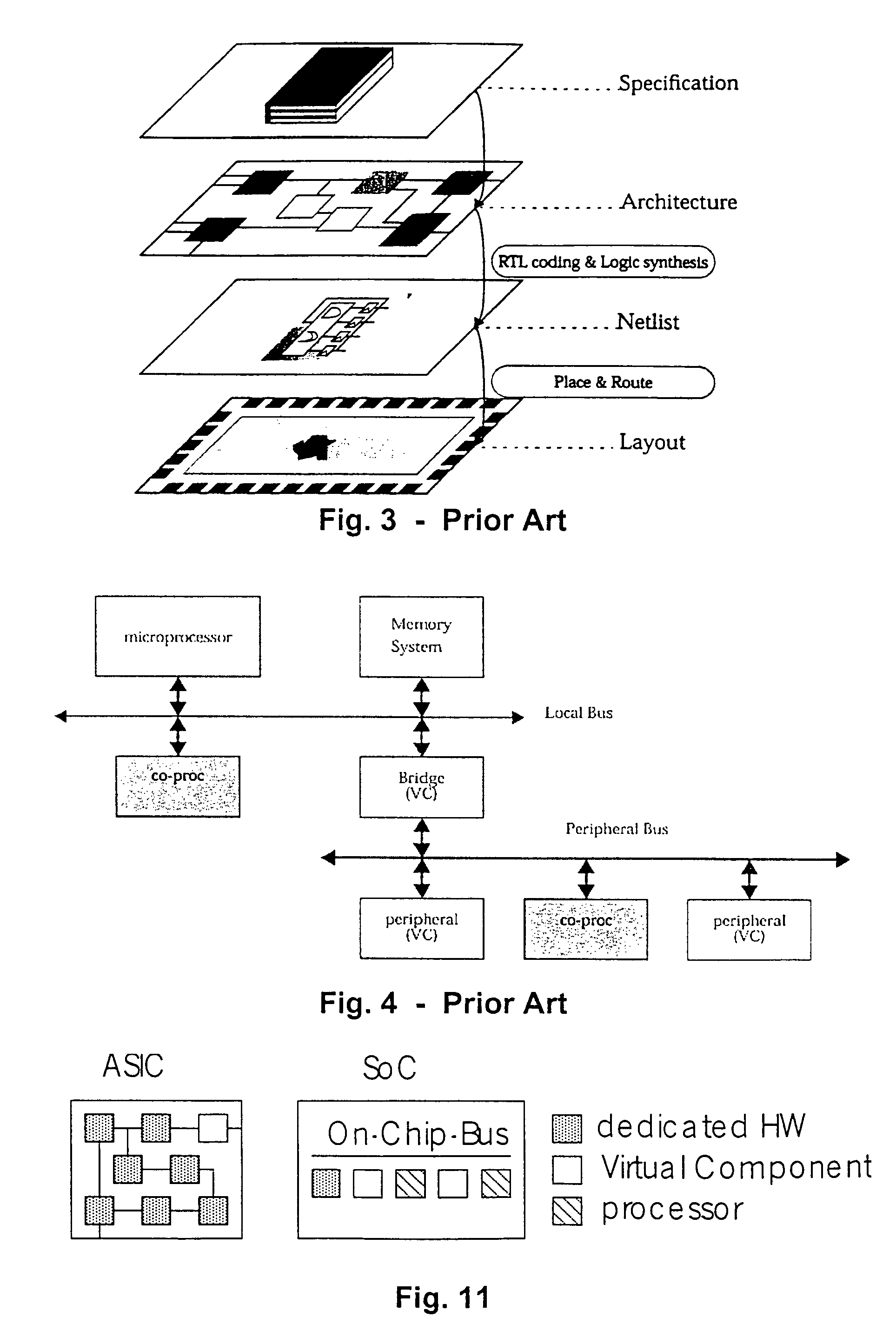
An interconnection network based on busses, such as the one shown in FIG. 4 requires the use of a shared medium for exchanging messages and has several drawbacks:A network based on a single shared medium does not scale well with the number of clients because the shared medium saturates and becomes the bottleneck when new clients are added.Long busses create several technological problems, such as excessive capacitive load which are a potential source of ramp-time errors, spreading of the clock skew problem over the entire chip.
These problems are expected to become even worse in deep sub-micron VLSI technology.With deep sub-micron technology, the main source of delay is interconnection delay.
Long busses will be the main source of performance degradation.
Therefore, wire delays become dominant.

Method used


Image

  • Array of parallel programmable processing engines and deterministic method of operating the same
  • Array of parallel programmable processing engines and deterministic method of operating the same
  • Array of parallel programmable processing engines and deterministic method of operating the same

Examples


example 1

FIR Filter

[0263]The filter in this example is a linear phase 32-tap FIR filter for 16-bit samples and 12 bit coefficients. The result is saturated at + / −219 and then scaled by 0, −6, −12 or −18 dB. The FIR filter concept is shown in FIG. 17, and an FIR implementation diagram is shown in FIG. 18.

[0264]Several alternatives have been investigated all of which represent embodiments of the present invention:[0265]Solution 1: All the operations are performed using the basic instruction set of the generic ASIP. All multiplications are expanded into a series of shifts and additions.[0266]Solution 2: with MAC co-processor: A coprocessor has been added to the processor to perform the multiply-accumulate operation. It is mapped into the processors memory space, and occupies 4 addresses: one to initialize the accumulator register, one to set the first operand, one to set the second operand and to trigger the multiply-accumulate operation, and one to read back the accumulator register.[0267]Solu...

example 2

CRC Encoder

[0277]This example calculates the USB data CRC on an incoming bitstream divided in frames of 3200 bits. After every frame the CRC is appended to the data stream. The incoming and outgoing data are organized in 32-bit words. A functional diagram of a CRC encoder example is shown in FIG. 19.

[0278]Two alternatives have been investigated:[0279]Solution 1: The first alternative is a pure software solution. Delay line and coefficients are implemented in the processors 32 bit numeric type, which allows an efficient implementation.[0280]Solution 2: The CRC extension unit contains a 32-bit CRC register and a 32-bit coefficient register. It is able to update the CRC register for 8 subsequent data bits (the 8 lowest bits of the argument) in one clock cycle. The return value is the argument shifted to the right by 8 bit positions. So the CRC can be updated for a 32-bit argument by invoking the CRC update instruction 4 times. Besides the CRC update instructions, the unit also contains...

example 3

Reed Solomon Encoder

[0284]Reed Solomon encoding follows a scheme similar to a CRC calculation. However, while the ‘typical’ CRC circuit operates on bits, the Reed Solomon Encoder processes multiple bits (in the present case 8). The CRC AND is replaced by a Galois Field multiplication and the XOR by a Galois field addition. The datastream to be encoded is divided in blocks—239 bytes in the case of this example. After initialisation of the delay line to all zeros, each byte of the datablock is fed into the encoder. At the end, the content of the delay line (16 bytes) is appended to the datablock. The incoming bytes are interpreted as the polynomial representation of a number in GF(28) (i.e.: the bits of the data are the coefficients of the polynomial). A functional diagram of the RS encoder is given in FIG. 20, and an implementation diagram is given in FIG. 21.

[0285]Several alternatives have been investigated:[0286]Solution 1: Software-only solution: The GF(28) addition is implemented...


PUM


Abstract

The present invention provides an array of parallel programmable processing engines interconnected by a switching network. At least some of the processing engines execute a thread, and at least some threads communicate with each other through communication objects either internally within one processing engine or through the network. A scheduling step of the parallel programmable processing engines is initiated by one or more events, an event being defined by a change of a state variable of a communication object. The array comprises:means for scheduling a scheduling step of the processing engines, the scheduling means comprising means for executing at least a first set of threads in parallel,means for updating state values of communications objects in response to the parallel executing step, andmeans for repeatedly and sequentially scheduling the executing means and the updating means until no more events occur.The present invention also provides a deterministic method of operating such an array.

Description

TECHNICAL FIELD OF THE INVENTION[0001]The present invention relates to a method of operating an array of parallel programmable processing engines interconnected by a switching network, as well as to such an array of parallel programmable processing engines and software related thereto.BACKGROUND OF THE INVENTION[0002]The task of an IC (Integrated Circuit) designer is to translate a specification of an integrated circuit into an implementation, such that all requirements are satisfied and all design objectives are optimised.[0003]IC design can also be described more formally as follows. The specification of a system is described in a language Lspecification, which contains the system's functionality, requirements and design objectives. Typically, this language is a combination of plain English, high level programming languages and mathematical formulae. Further a design language Ldesign is provided, primitive design elements of which correspond to existing (or automatically generated...

Claims


Application Information

Patent Timeline
IPC IPC(8): G06F9/46G06F9/50G06F17/50
CPCG06F9/5066G06F9/30014G06F17/5045G06F17/5022G06F30/30G06F30/33G06F30/3308G06F2117/04
Inventor VANDEWEERD, IVO
Owner TRANSWITCH
Learn More