Light emitting device, electronic device, and television device

a technology of light emitting devices and electronic devices, applied in the field of semiconductors, to achieve the effects of reducing the luminance by half, good luminous efficiency, and enhancing color purity

Inactive Publication Date: 2008-08-26
SEMICON ENERGY LAB CO LTD
View PDF31 Cites 25 Cited by
  • Summary
  • Abstract
  • Description
  • Claims
  • Application Information

AI Technical Summary

Benefits of technology

[0014]A so-called color filter is formed of colored layers of red, green, and blue regularly arranged over a substrate integrated with a black matrix adjacent arranged therebetween. In the case of forming a color filter by a printing method, a colored layer and a black matrix overlap partly and a thick part to be depressions on the surface is formed if a black matrix is formed, and thereafter, colored layers of red, green, and blue are formed so as not to make an empty space. In addition, a partially overlapped part is made and a thick part is also formed even if colored layers of red, green, and blue are first formed and a black matrix is then formed. Therefore, the conventional color filter has a transparent layer referred to as an overcoat layer for making the depressions flat. The overcoat layer increases a total thickness of a color filter.
[0042]In addition, the quantity of a filler between a pair of substrates can be reduced if the space between the substrates is narrowed. The space between a pair of substrates can be filled well with the filler by forming a base layer for improving adhesion, even if the space between the substrates is narrowed. The base layer for improving the adhesion enables the fixing intensity between a pair of substrates to be enhanced and reliability of a light emitting device to be improved.

Problems solved by technology

In the case of manufacturing a full-color flat panel display using emission colors of red (R), green (G), and blue (B), a space between different pixels is designed to be wide or an insulator referred to as a bank (or a barrier) is disposed between pixels since the film formation by the above-described film formation method is not so accurate.

Method used


Image

  • Light emitting device, electronic device, and television device
  • Light emitting device, electronic device, and television device
  • Light emitting device, electronic device, and television device

Examples


embodiment 1

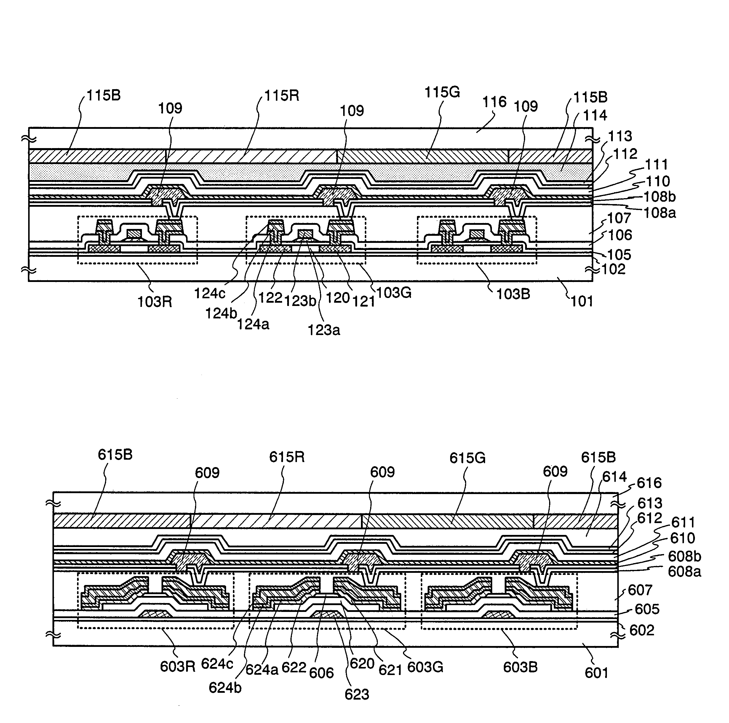
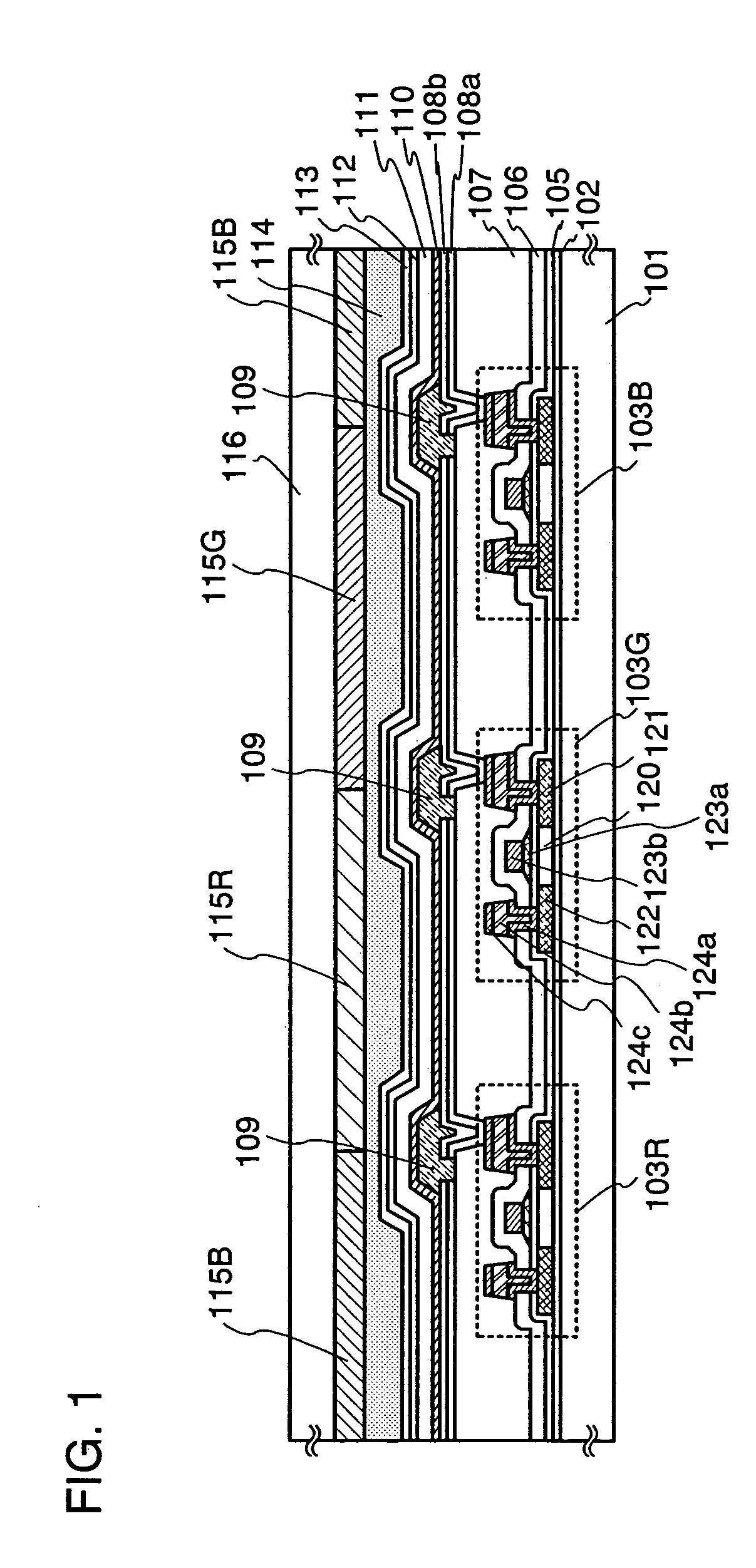
[0083]This embodiment describes an embodiment of manufacturing a top-emission type light emitting device with reference to FIG. 5A

[0084]First, a base insulating film is formed over a first substrate 401. Any substrate with planarity and thermostability may be adopted as the first substrate 401, without being particularly limited. As the base insulating film, a base film made of an insulating film such as a silicon oxide film, a silicon nitride film, or a silicon oxynitride film is formed.

[0085]Next, a semiconductor film is formed over the base insulating film. A semiconductor layer is formed as described below. A semiconductor film having an amorphous structure is formed by a known method (a sputtering method, a LPCVD method, a plasma CVD method, or the like). Thereafter, a known crystallization processing (a laser crystallization method, a thermal crystallization method, a thermal crystallization method with a catalyst such as nickel, or the like) is performed, thereby obtaining a ...

embodiment 2

[0110]An example of manufacturing a dual-emission type light emitting device is described in this embodiment with reference to FIG. 5B.

[0111]First, a base insulating film is formed over a light-transmitting first substrate 501. Any substrate with a light-transmitting property may be adopted as the first substrate 501. As a base insulating film, a base film made of an insulating film such as a silicon oxide film, a silicon nitride film, or a silicon oxynitride film is formed.

[0112]A semiconductor layer is formed over the base insulating film as in Embodiment 1. A gate insulating film for covering the semiconductor layer is formed and a gate electrode is formed thereon as in Embodiment 1.

[0113]An n-type lightly doped impurity region, a p-type heavily doped impurity region, an n-type heavily doped impurity region, or the like is formed by doping as in Embodiment 1. Then, a resist mask is removed and an insulating film including hydrogen (a light-transmitting interlayer insulating film)...

embodiment 3

[0132]An example of manufacturing a light emitting device using a bottom gate type (inversely staggered) TFT is described in this embodiment with reference to FIG. 6.

[0133]First, a base insulating film 602 is formed over a substrate 601. It is preferable to use an insulating film such as a silicon oxide film, a silicon nitride film, or a silicon oxynitride film (SiOxNy) as the base insulating film 602. Note that the substrate 601 can adopt a plastic substrate with the thermostability that can withstand a processing temperature in this manufacturing process, or the like, besides a non-alkaline glass substrate.

[0134]A conductive film of 100 to 600 nm in a film thickness is formed over the base insulating film 602. An element which is selected from Tantalum (Ta), titanium (Ti), molybdenum (Mo), tungsten (W), chromium (Cr), silicon (Si), scandium (Sc), Nd, Al, or Cu, or an alloy film in which the elements are combined (typically, a Mo—W alloy and a Mo—Ta alloy) can be used for a conduct...


PUM


Abstract

A full-color flat panel display using emission colors of red, green, and blue is increasingly required to have higher definition, higher aperture ratio and higher reliability. A light emitting device of the invention has an insulator referred to as a bank, that is, a black matrix (BM), between pixels on a substrate side where a light emitting element and a TFT are disposed, and has colored layers of red, green, and blue on a sealing substrate side. This enables right and left margins of a pixel to be taken and a width of the bank to be 30 μm or less, preferably, 5 μm to 20 μm.

Description

BACKGROUND OF THE INVENTION[0001]1. Field of the Invention[0002]The present invention relates to a semiconductor device having a circuit including a thin film transistor (hereinafter, referred to as a TFT) and a manufacturing method thereof. For example, the invention relates to an electronic device equipped with a light emitting display device having a TFT and an organic light emitting element, as a part.[0003]Note that in this specification, a semiconductor device means overall devices which can function by using semiconductor properties. An electro-optical device, a semiconductor circuit and an electronic device are all included in the semiconductor device.[0004]2. Description of the Related Art[0005]Recently, research on a light emitting device having an EL element as a self-luminous light emitting element has been activated. This light emitting device is also referred to as an organic EL display or an organic light emitting diode. The light emitting device has characteristics s...

Claims


Application Information

Patent Timeline
Patent Type & Authority Patents(United States)
IPC IPC(8): H01J1/62H01L27/32H01L51/50H01L51/52
CPCH01L27/322H01L27/3246H01L51/5237H01L27/3213H01L51/5016H01L2251/5323H01L51/5284H01L2251/5315H01L51/5036H10K59/351H10K59/38H10K59/122H10K50/125H10K50/11H10K2101/10H10K50/841H10K50/865H10K2102/3031H10K2102/3026H10K50/844H05B33/22
Inventor YAMAZAKI, SHUNPEI
Owner SEMICON ENERGY LAB CO LTD
Why Eureka
Try Eureka