Phase-locked loop circuit, delay locked loop circuit, timing generator, semiconductor test instrument, and semiconductor integrated circuit

a phase lock and loop circuit technology, applied in pulse manipulation, pulse technique, instruments, etc., can solve the problems of poor linearity of vco voltage (or delay voltage), large power consumption, and deterioration of phase lock accuracy, so as to improve practical accuracy, reduce errors, and improve reliability

Inactive Publication Date: 2009-02-17
ADVANTEST CORP
View PDF11 Cites 20 Cited by
  • Summary
  • Abstract
  • Description
  • Claims
  • Application Information

AI Technical Summary

Benefits of technology

[0024]To achieve this aim, according to the present invention, there is provided a phase-locked loop circuit (PLL) comprising: feedback means for outputting an output signal which is a binary signal as a feedback signal; a phase comparator which receives the feedback signal and an input signal and outputs a phase signal representing a lead or a delay of a phase of the feedback signal relative to the input signal; a counter which receives the phase signal, increases a value in the control signal when the phase signal has a value representing a lead of the phase, and decreases the value in the control signal when the phase signal has a value representing a lag of the phase; and a ring oscillator which receives the control signal, produces the output signal, prolongs an oscillation cycle of the output signal when the number of values in the control signal is large, and shortens the oscillation cycle of the output signal when the number of values is small.
[0025]More specifically, the present invention has a structure in which the feedback means comprises a frequency divider; the frequency divider divides the output signal which is the binary signal and outputs a feedback signal which is the binary signal; the phase comparator receives the feedback signal and the input signal, detects a value of the feedback signal in synchronization with the input signal and outputs a detection result as a phase signal representing a lead or a lag of a phase of the feedback signal compared to the input signal; the counter receives the phase signal, outputs a control signal comprising a plurality of bits each of which represents a first value or a second value, increases the number of bits representing the first value in the control signal by one when the phase signal has a value representing a lead of the phase, and decreases the number of bits representing the first value in the control signal by one when the phase signal has a value representing a lag of the phase; and the ring oscillator receives the control signal, produces the output signal, prolongs the oscillation cycle of the output signal when the number of bits representing the first value in the control signal is large and shortens the oscillation cycle of the output signal when the number of bits representing the first value is small.
[0026]According to such a digital-controlled PLL of this invention, by providing a circuit configuration based on logic elements without using analog circuits, a reduction in power consumption, size of a circuit scale and cost can be achieved. Furthermore, according to the PLL of the present invention, since an analog circuit whose response speed is low is not used, especially an LPF is not used, a phase can be locked with the high accuracy in a higher band. Therefore, a lock loop band can be improved. Moreover, according to the PLL of the present invention, in the phase comparator, a lead or a lag of a phase is detected as a value of the feedback signal in synchronization with the input signal irrespective of a phase difference. Therefore, the reliability of the phase comparison can be improved. Additionally, in the present invention, since a priority encoder type counter which increases / decreases the number of bits representing the first value in the control signal by one based on the phase signal is used, only the value of one bit is changed at a time in the control signal. Thus, the reliability can be improved.

Problems solved by technology

When an SR latch is utilized for the phase comparator in particular, the linearity of the VCO voltage (or the DELAY voltage) is especially poor in the vicinity of a point where the phase difference is zero as shown in FIG. 28.
Therefore, in the conventional PLL or DLL, there is a problem that the accuracy of the phase lock is deteriorated.
Therefore, there are problems that a power consumption is large, a circuit scale is increased and a cost is high.
For example, a circuit in which an OP amplifier is used for the phase comparator has large power consumption and is hard to be reduced in size.
Further, a circuit in which PMOS and NMOS analog switches and an OP amplifier are used for the charge pump also has large power consumption and is hard to be reduced in size.
Furthermore, in regard to a regulator which changes a voltage variable range of the VCO or the DELAY, a power consumption becomes large when an operating speed is increased, and a dimension of the regulator also becomes large.
Therefore, this can be an obstacle in increasing a lock loop frequency band.
Moreover, since the analog circuit includes a circuit whose response speed is low such as an OP amplifier or an LPF, it is hard to perform phase locking with the high accuracy in a high frequency band in the PLL or DLL using the conventional analog circuit.
However, in a large-scale chip such as a logic circuit, there is a problem that a skew is generated between parts distanced from each other on the chip due to irregularities in characteristics of relay buffers for clock signals.
Therefore, a so-called whisker may be applied to a selector of the delay circuit, which may possibly lead to a malfunction.

Method used


Image

  • Phase-locked loop circuit, delay locked loop circuit, timing generator, semiconductor test instrument, and semiconductor integrated circuit
  • Phase-locked loop circuit, delay locked loop circuit, timing generator, semiconductor test instrument, and semiconductor integrated circuit
  • Phase-locked loop circuit, delay locked loop circuit, timing generator, semiconductor test instrument, and semiconductor integrated circuit

Examples


first embodiment

[0092]First, an example of a phase-locked loop circuit (PLL) according to the present invention will be described as a first embodiment.

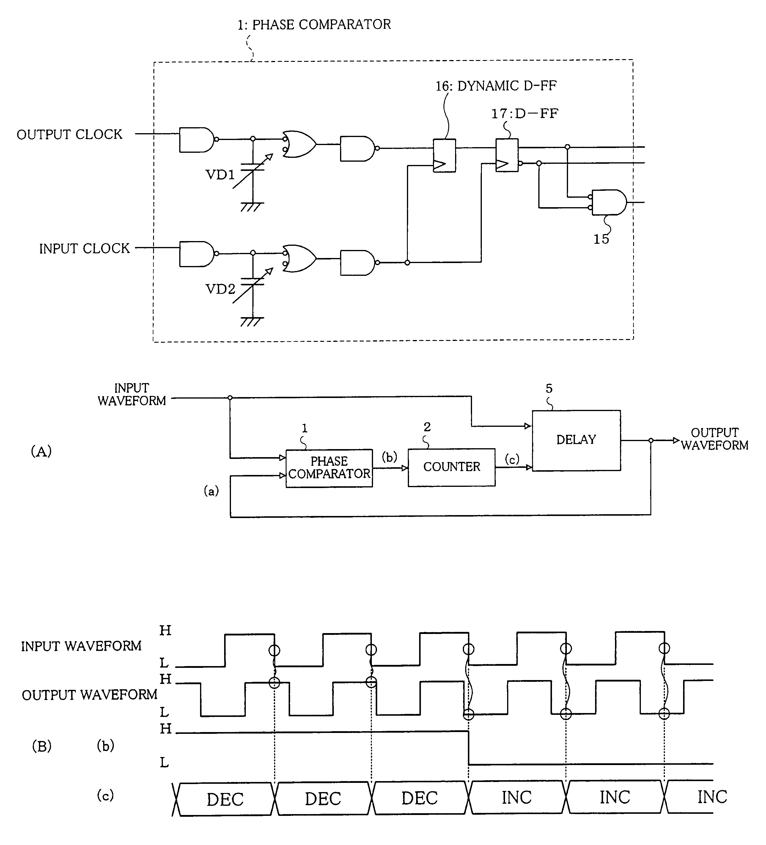
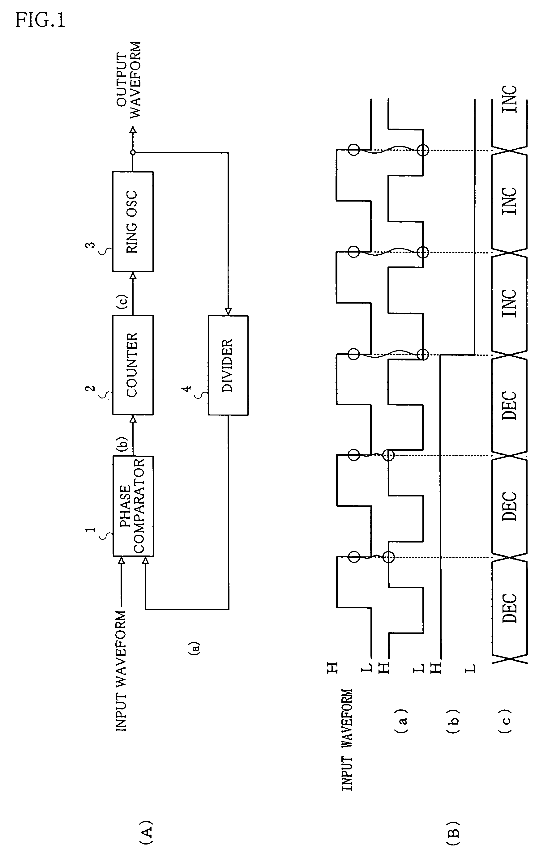
[0093]As shown in FIG. 1(A), a PLL according to the first embodiment comprises a phase comparator 1, a counter 2, a ring oscillator (RING OSC) 3, and a frequency divider 4. Further, in the PLL, an output signal (output waveform) as a binary signal of the ring oscillator 3 is divided by the frequency divider 4, and inputted to the phase comparator 1 as a feedback signal as a binary signal which is “H” or “L”.

[0094]To the phase comparator 1 is inputted an input signal (input waveform) together with the feedback signal. Then, the phase comparator 1 detects a value of the feedback signal in synchronization with the input signal. In this embodiment, as shown in FIG. 1(B), the phase comparator 1 samples a value of the feedback signal with a timing of a trailing edge of the input signal.

[0095]Subsequently, the phase comparator 1 outputs a detection result ...

second embodiment

[0129]Another example of the PLL according to the present invention will now be described as a second embodiment with reference to FIG. 5.

[0130]In the second embodiment, respective constituent components other than the ring oscillator 3 are the same as those in the above-described first embodiment, thereby eliminating their explanation.

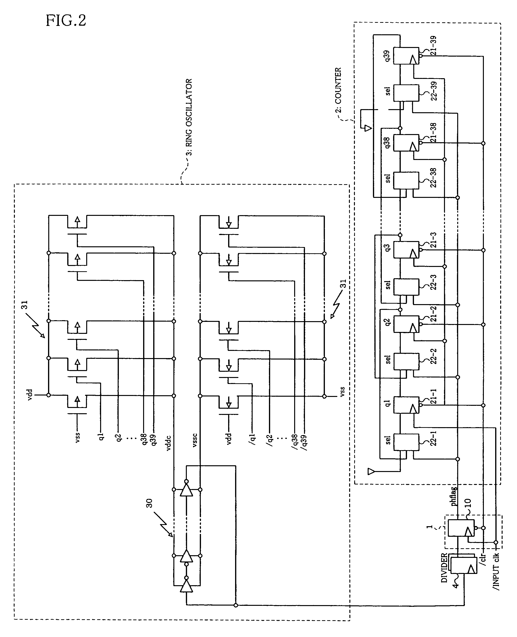
[0131]The ring oscillator 3 according to the second embodiment comprises inverters 30 connected in series on multiple stages like the first embodiment. Moreover, it comprises variable capacitances 32 provided between the respective inverters 30 and a grounded voltage source.

[0132]Additionally, the respective variable capacitances 32 comprise load capacitances 322 whose number is equal to the number of bits in the control signal and which are connected with each other in parallel, and switching elements 321 which are connected with the respective load capacitances 322 in series.

[0133]Here, a gate capacitance of the transistor is utilized as the load ca...

third embodiment

[0136]Still another example of the PLL according to the present invention will now be described as a third embodiment.

[0137]Like the above-described first and second embodiments, the digital-controlled PLL can reduce a cycle clock number required until feedback is applied after passing a lock target as compared with a conventional analog-controlled PLL. As a result, a loop lock band can be increased.

[0138]Meanwhile, in a D flip-flop such as shown in FIG. 6(A), a phase difference when an output value is switched from “H” to “L” from a timing to detect a division signal such as shown in FIG. 6(B) may not be necessarily equal to a phase difference when the output value is switched from “L” to “H” in some cases.

[0139]In such a case, as shown in FIG. 6(C), there may be generated hysteresis that a phase difference between a feedback signal such as a data signal and an input signal such as a clock signal differs depending on a change direction of an output value of the D flip-flop. In part...


PUM


Abstract

A PLL and DLL are designed such that the power consumption is reduced, the size is reduced, the band width of the locked loop is increased, and the reliability is improved. There are provided a phase comparator for measuring the value of a feedback signal in synchronism with an input signal and outputting a phase signal representing the lead or lag of the phase of the feedback signal, a counter for increasing by one the number of bits representing “H” in a control signal when the phase signal represents the lead of the phase or decreasing by one the number of bits representing “H” in the control signal when the phase signal represents the lag of the phase, and a ring oscillator for increasing the oscillation period when the number of bits representing “H” in the control signal increases or decreasing the oscillation period when the number of bits representing “H” decreases.

Description

TECHNICAL FIELD[0001]The present invention relates to a digital-controlled phase-locked loop circuit (PLL) comprising logic elements, a delay locked loop circuit (DLL), a timing generator utilizing the DLL, a semiconductor test instrument including the timing generator, and a semiconductor integrated circuit equipped with the PLL.BACKGROUND ART[0002]Prior to explaining the present invention, a constitution of a conventional general PLL will be described.[0003]As shown in FIG. 24(A), a conventional PLL comprises a phase comparator 101, a charge pump 102, a low pass filter (LPF) 103, a voltage controlled oscillator (VCO) 104, and a frequency divider 105.[0004]As shown in FIGS. 24(A) and (B), the phase comparator 101 compares an input waveform with a divided waveform obtained by dividing an output waveform of the VCO 104 by the frequency divider 105. Further, it performs an operation to detect how much a phase of the divided waveform is delayed from a phase of the input waveform, and a...

Claims


Application Information

Patent Timeline
Patent Type & Authority Patents(United States)
IPC IPC(8): H03L7/06H03K5/13H03K5/131H03L7/081H03L7/089H03L7/093H03L7/099
CPCH03L7/0814H03L7/089H03L7/093H03L7/0995H03L7/0816H03L7/099
Inventor SUDA, MASAKATSU
Owner ADVANTEST CORP
Why Eureka
Try Eureka