Method for manufacturing p-type group III nitride semiconductor, and group III nitride semiconductor light-emitting device

a technology of nitride semiconductor and nitride, which is applied in the direction of semiconductor lasers, crystal growth process, polycrystalline material growth, etc., can solve the problems of reduced crystallinity, difficult formation of p-type semiconductors, and high cost, and achieves fewer steps and better productivity.

Active Publication Date: 2009-05-26
TOYODA GOSEI CO LTD
View PDF7 Cites 3 Cited by
  • Summary
  • Abstract
  • Description
  • Claims
  • Application Information

AI Technical Summary

Benefits of technology

[0008]The present invention was developed in order to overcome the abovementioned drawbacks of the prior art, and an object of the present invention is to provide a method for manufacturing a p-type group III nitride semiconductor that has adequate carrier concentration and a surface with a low occurrence of crystal damage.
[0022]By the present invention, a p-type group III nitride semiconductor having a p-type carrier concentration sufficient to enable its use as a semiconductor device can be manufactured without deteriorating the morphology of the top surface of the group III nitride semiconductor layer and without damaging the crystallinity of the top surface. The method of the present invention also has fewer steps and better productivity in comparison with the activation annealing by the conventional method because the material is converted to the p-type by a treatment carried out after growth has been completed in the growth apparatus.

Problems solved by technology

It has been difficult to form a p-type semiconductor that has an adequate carrier concentration from a group III nitride semiconductor.
However, the step for removing the group III nitride semiconductor from the growth apparatus and performing post-processing is complex in the abovementioned method, and the cost is high.
This method also has drawbacks in that the crystallinity is reduced by the heat treatment because nitrogen is desorbed at the same time as dehydrogenation is performed by the heat treatment, and that the luminous intensity is low in the light-emitting device created using this method.
However, nitrogen substitution is performed in a vacuum in this method, nitrogen is desorbed from the crystal, perhaps due to the vacuum state, and crystallinity is reduced.
However, substitution with an inert gas is performed at 1100° C. in this method, which is the growth temperature of the nitride semiconductor, so nitrogen is desorbed from the crystal, and crystallinity declines.

Method used


Image

  • Method for manufacturing p-type group III nitride semiconductor, and group III nitride semiconductor light-emitting device
  • Method for manufacturing p-type group III nitride semiconductor, and group III nitride semiconductor light-emitting device

Examples


example 1

[0043]In the present example, a sample was fabricated by a process in which a GaN layer was formed as a buffer layer, on a sapphire substrate using the MOCVD method, and a GaN layer doped with Mg was laminated thereon at 1100° C. Furthermore, after lamination, the supply of ammonia gas and H2 was stopped at a temperature of 1050° C., nitrogen gas was supplied thereto instead, and the product was cooled, whereby an Mg p-type dopant was put in an activated state. Details thereof are described hereinafter.

[0044]The sample with a GaN layer was fabricated using the MOCVD method in the procedure described below. First, the sapphire substrate was inserted into a quartz reactor mounted in the RF coil of an induction heating furnace. The sapphire substrate was placed on a carbon susceptor used for heating. After the substrate had been inserted, a vacuum was formed inside the reactor, the air was removed, nitrogen gas was circulated therein, and the inside of the reactor was purged. After the...

example 2

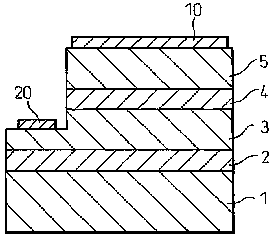
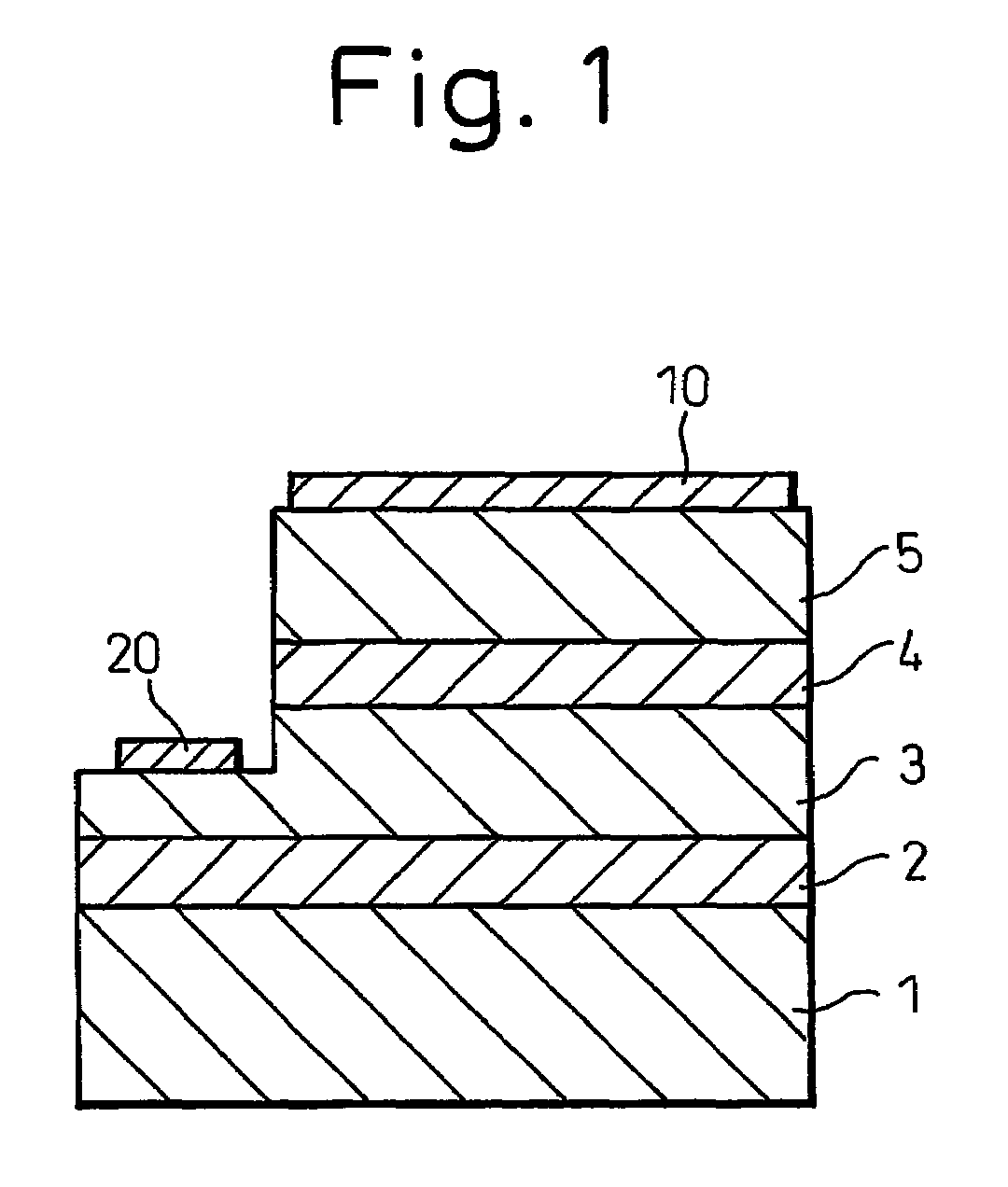
[0060]The group III nitride semiconductor light-emitting device depicted in FIG. 1 was fabricated using the p-type group III nitride semiconductor obtained by the manufacturing method of the present invention.

[0061]An n-type semiconductor layer 3, a light-emitting layer 4, and a p-type semiconductor layer 5 were grown in this order by a common vacuum MOCVD method widely known in the art via a buffer layer 2 composed of AlN on a substrate 1 composed of a sapphire c face ((0001) crystal face), and a layered structure was fabricated. An undoped GaN layer (foundation layer: layer thickness=2 μm) and a Ge-doped n-type GaN layer (n contact layer: layer thickness=2 μm, carrier concentration=1×1019 cm−3) were laminated in the same order as the n-type semiconductor layer 3. The light-emitting layer 4 had a multiple quantum structure composed of a six-layer Ge-doped GaN barrier layer (layer thickness=14.0 nm, carrier concentration=1×1018 cm−3) and a five-layer undoped In0.20Ga0.80N well layer...

example 3

[0075]A light-emitting device was fabricated in the same manner as Example 2, except that a translucent positive electrode having the ability to transmit light from the blue to ultraviolet range and formed by layering a nickel (Ni) film / gold (Au) film was used as the positive electrode and the metal film in contact with the p contact layer 5 was constituted by a nickel film.

[0076]The sapphire surface of the light-emitting device thus obtained was then attached to a mount, the negative electrode and positive electrode were connected to a lead frame by gold wires, and the product was evaluated in the same manner as in Example 2.

[0077]The forward drive voltage (Vf) was 3.0 V when the forward current was set to 20 mA, the light output measured by a common integrating sphere was 6 mW, and the wavelength of the emitted light was 455 nm. The reverse voltage (Vr) was 20 V or higher when the reverse current was set to 10 μA. Approximately 10,000 LED chips, not counting products defective in ...


PUM

PropertyMeasurementUnit
temperatureaaaaaaaaaa

Abstract

An object of the present invention is to provide an efficient method for manufacturing a p-type group III nitride semiconductor that has adequate carrier concentration and a surface with a low occurrence of crystal damage. The inventive method for manufacturing a p-type group III nitride semiconductor comprises: (a) growing a group III nitride semiconductor containing a p-type dopant at 1000° C. or higher in an atmosphere containing H2 gas and / or NH3 gas; and (b) after the growth of the group III nitride semiconductor, substituting the H2 gas and NH3 gas with an inert gas at a temperature higher than 800° C. while reducing the temperature.

Description

CROSS REFERENCE TO RELATED APPLICATION[0001]This application is an application filed under 35 U.S.C. §111(a) claiming benefit pursuant to 35 U.S.C. §119(e)(1) of the filing date of the Provisional Application No. 60 / 519,636 filed on Nov. 14, 2003, pursuant to 35 U.S.C. §111(b).TECHNICAL FIELD[0002]The present invention relates to a method for manufacturing a p-type group III nitride semiconductor and to a group III nitride semiconductor light-emitting device using the same and, particularly, relates to a method for manufacturing a p-type group III nitride semiconductor that is formed in layers on the surface of a substrate and that has an adequate carrier concentration and a surface with a low occurrence of crystal damage.BACKGROUND ART[0003]Group III nitride semiconductor materials have recently garnered attention as semiconductor materials used in light-emitting devices for emitting short-wavelength light. A group III nitride semiconductor is generally formed in layers by metal or...

Claims


Application Information

Patent Timeline
Patent Type & Authority Patents(United States)
IPC IPC(8): H01L21/00C01G15/00H01L21/20H01L21/205H01L33/00H01L33/06H01L33/32H01L33/42H01S5/323
CPCC30B25/02C30B29/403C30B29/406H01L21/0237H01L21/02458H01L33/007H01L21/02579H01L21/0262H01L21/0254H01L21/02543H01L21/02546
Inventor KOBAYAKAWA, MASATO
Owner TOYODA GOSEI CO LTD
Why Eureka
Try Eureka