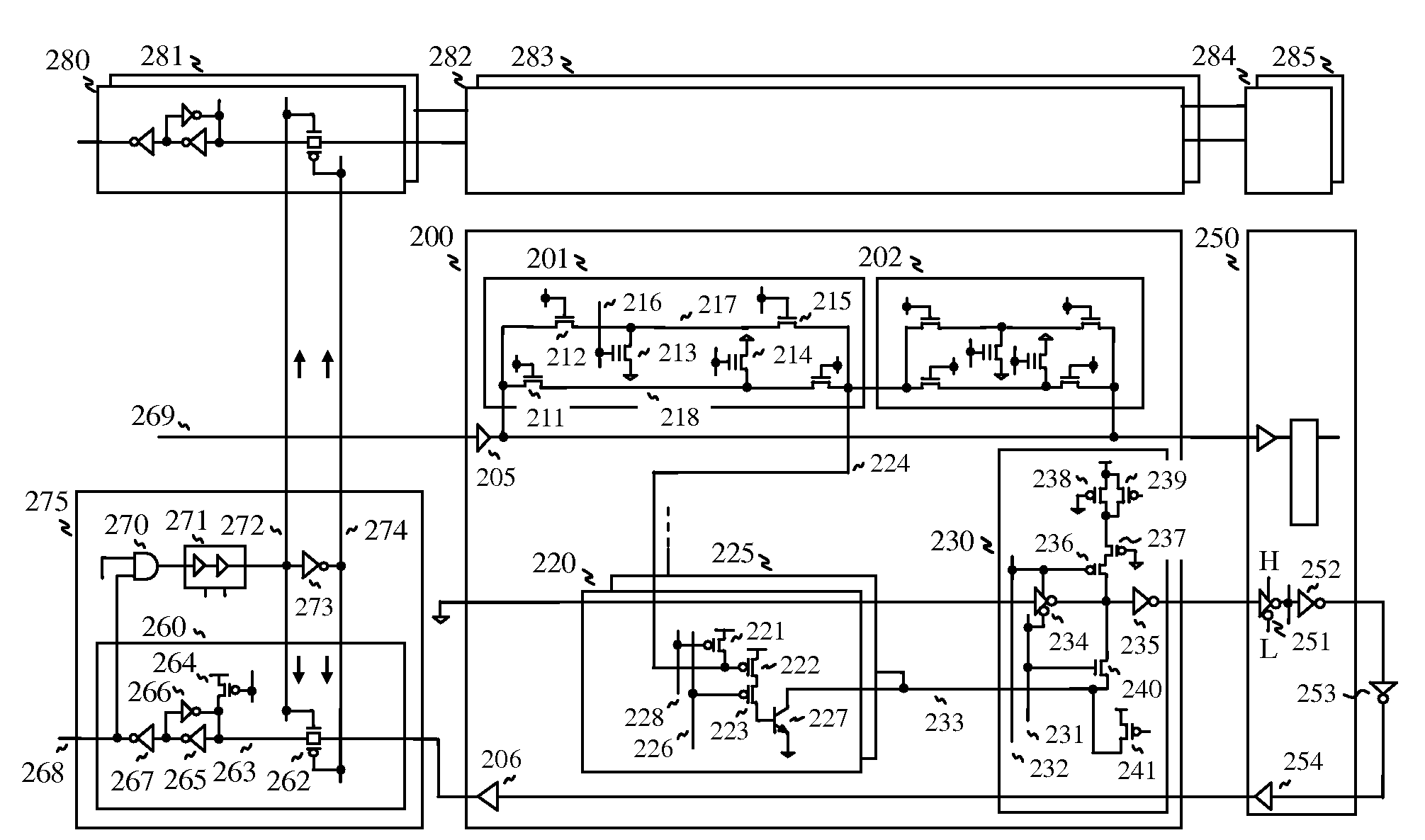
[0012]In the present invention, NOR
flash memory including bipolar read circuit is described. By introducing multi-divided bit line architecture, bit line loading is reduced. Thus, the bit line is quickly discharged by a selected cell transistor. In particular, a bipolar segment read circuit is added to amplify the bit line voltage in order to obtain higher
gain, which realizes to read the cell transistor more effectively, even though the cell transistor can flow relatively low current. The bipolar segment read circuit is composed of a few MOS transistors and a bipolar transistor, in order to insert within the memory cell array repeatedly. And, the cell transistor can be formed from
single crystal silicon or thin film
polycrystalline silicon because the lightly load bit line can be driven by the cell transistor even though the cell transistor can flow relatively low current, which also realizes multi-stacked flash memory with
low temperature polycrystalline silicon. With low temperature process, routing
metal layers and cell transistors in the bottom are not affected when
processing the upper cell transistors. Furthermore, the cell transistor can be miniaturized further. As a result, the present invention can overcome the scaling limit of the conventional planar
CMOS process. There are almost no limits to stack multiple memory cells as long as the flatness is enough to accumulate the transistors.
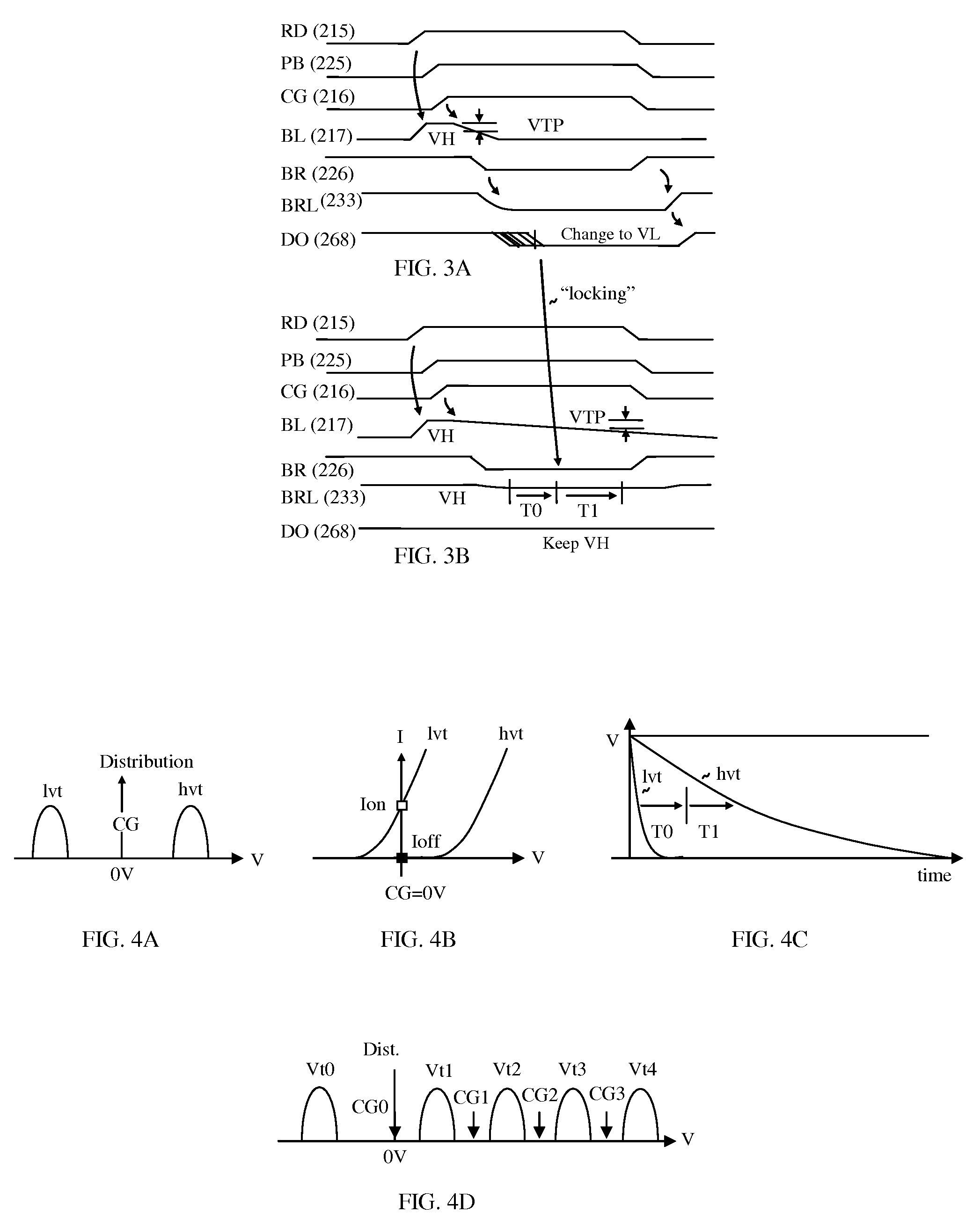
[0015]And a delay circuit is added for generating the locking signal from the reference signal because there is a need for adding predetermined
delay time before locking the latch circuit with the statistical data for all the memory cells such as mean time between low threshold data and high threshold, in order to compensate cell-to-cell variations. Thereby the delay circuit generates a delay for optimum range of locking time, which circuit is tunable. The read output from the cell transistor is transferred to the latch circuit through a returning read path, thus the
access time of the cell transistor is equal regardless of the location of the cell transistor, which is advantageous to transfer the read output to the external pad at a time.
[0016]The time-domain sensing scheme effectively differentiate low threshold data and high threshold data with time delay control, while the conventional sensing scheme is current-domain or voltage-domain sensing scheme. In the convention memory, the cell current is converted to voltage, and the voltage is compared by a
comparator or an
inverter, so that there is not much choice to control the
comparator with existing circuits, because current and voltage are directly related to the process parameters. Now in the present invention, there is one more converting step to read the data, such that the current of the cell transistor discharges the bit line, the segment read circuit detects the voltage of the bit line, and the voltage data is converted to
time difference by the block read circuit. Furthermore, the block read circuit is tunable to differentiate low threshold data and high threshold data more effectively. As a result, the read output of the block read circuit is reached to the latch circuit through the returning
data path. In doing so, the low threshold data is reached to the latch circuit earlier, while high threshold data is rejected by the locking signal. There are many advantages to adopt the time-domain sensing scheme, so that the sensing time is easily controlled by the tunable delay circuit, which compensates
wafer-to-
wafer variation as well. Furthermore, this circuit technique is also useful for
small cell transistors, such as
nanocrystal memory and
single electron memory including
quantum dot, because
small cell transistors can flow very low current. Moreover, the bit line can be divided into a small piece for reducing
parasitic capacitance of the bit line, which enables the time-domain sensing scheme can differentiate very low current difference with lightly loaded bit line.
[0017]One more
advantage is that the time-domain sensing scheme is useful for reducing the cell current difference between the turn-on current of the low threshold data and the turn-off current of the high
threshold current. In the conventional flash memory, there is at least several 1000 times difference between the turn-on current and the turn-off current, in order to read the cell transistor with existing
comparator or an
inverter. In the present invention, the current difference can be reduced, for example, to several 100 times instead of several 1000 times, as long as the distribution of the difference is stable at a given fabrication process for manufacturing.

