Method of manufacturing semiconductor device

a manufacturing method and semiconductor technology, applied in capacitors, electrical appliances, capacitors with voltage varied dielectrics, etc., can solve the problems of flash memory, inability to meet the demand for higher performance of ferams, and relatively high voltage, so as to prevent the deterioration of ferroelectric characteristics and less prone to generation of hydrogen

Inactive Publication Date: 2009-06-23
FUJITSU SEMICON LTD
View PDF10 Cites 2 Cited by
  • Summary
  • Abstract
  • Description
  • Claims
  • Application Information

AI Technical Summary

Benefits of technology

[0019]In the present invention, the annealing of the first ferroelectric film causes impurities such as water and organic materials contained in the first ferroelectric film to be expelled to the outside of the film. Thus, it is made possible to provide a semiconductor device including a capacitor in which an increase in the switching charge amount, a decrease in the leakage current, a decrease in the fatigue, and an improvement in the imprint characteristics are simultaneously achieved.
[0020]Furthermore, since the second ferroelectric film is formed of the amorphous material or the microcrystalline material, elements of the second conductive film, which diffuse into the capacitor dielectric film, remain in the second ferroelectric film, and are less prone to reach the first ferroelectric film. As a result, the above-described elements are less prone to diffuse into grain boundaries of the first ferroelectric film which is crystallized to show excellent ferroelectric characteristics. Accordingly, leakage paths are prevented from being formed by the elements, and it is made possible to effectively prevent the leakage current of the capacitor.
[0023]The second metal oxide film thus containing a large amount of oxygen inhibits the catalysis of the second metal oxide film. Accordingly, even when external water is brought into contact with the second metal oxide film, hydrogen is less prone to be generated. Thus, it is made possible to prevent deterioration of ferroelectric characteristics of the first and second ferroelectric films, the deterioration stemming from reduction by hydrogen.
[0024]The first metal oxide film may be annealed in an oxygen-containing atmosphere after the step of forming the first metal oxide film and before the step of forming the second metal oxide film. This annealing compensates oxygen deficiency in the first and second ferroelectric films, and planarizes unevenness at the interface between the first metal oxide film and the second ferroelectric film.

Problems solved by technology

Therefore, the flash memory has a disadvantage that a relatively high voltage is needed.
However, the technologies described in Patent Documents 1 to 3 cannot simultaneously improve all of these characteristics, and cannot meet the demand for higher performance of FeRAMs.
The technology of Patent Document 1 cannot meet this demand for FeRAMs to have such a life that the switching charge amount does not decrease even when the number of polarization reversals becomes 1010 or more.
However, there arises another problem in which a process is complicated when a multilayer structure having three or more layers is employed.
However, as shown in FIG. 10 of Patent Document 3, there is a problem that the switching charge amount decreases due to the annealing of a ferroelectric film.

Method used


Image

  • Method of manufacturing semiconductor device
  • Method of manufacturing semiconductor device
  • Method of manufacturing semiconductor device

Examples


first embodiment

(1) First Embodiment

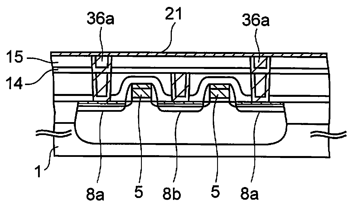
[0040]FIGS. 1A to 1W are cross-sectional views of a semiconductor device according to a first embodiment in the process of being manufactured.

[0041]This semiconductor device is a stack-type FeRAM advantageous in miniaturization, and is fabricated as follows.

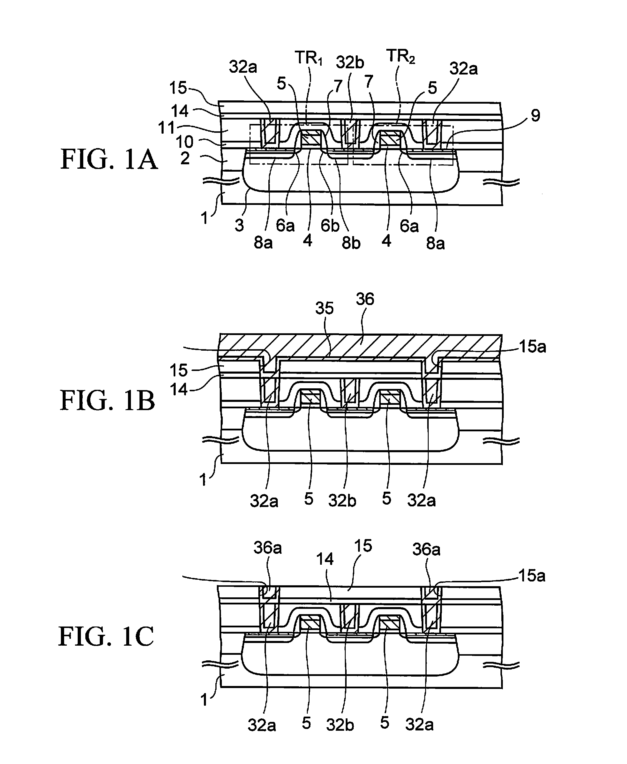
[0042]At the beginning, steps for obtaining the cross-sectional structure shown in FIG. 1A will be described.

[0043]First, on a surface of an n- or p-type silicon (semiconductor) substrate 1, a groove for shallow trench isolation (STI), which defines an active region for transistors, is formed, and the inside of the groove is filled with an insulating film made of silicon oxide or the like which is used as an element isolation insulating film 2. Incidentally, an element isolation structure is not limited to STI, and the element isolation insulating film 2 may be formed by local oxidation of silicon (LOCOS).

[0044]Next, a p-type impurity is introduced into the active region of the silicon substrate 1 to form a p-...

second embodiment

(2) Second Embodiment

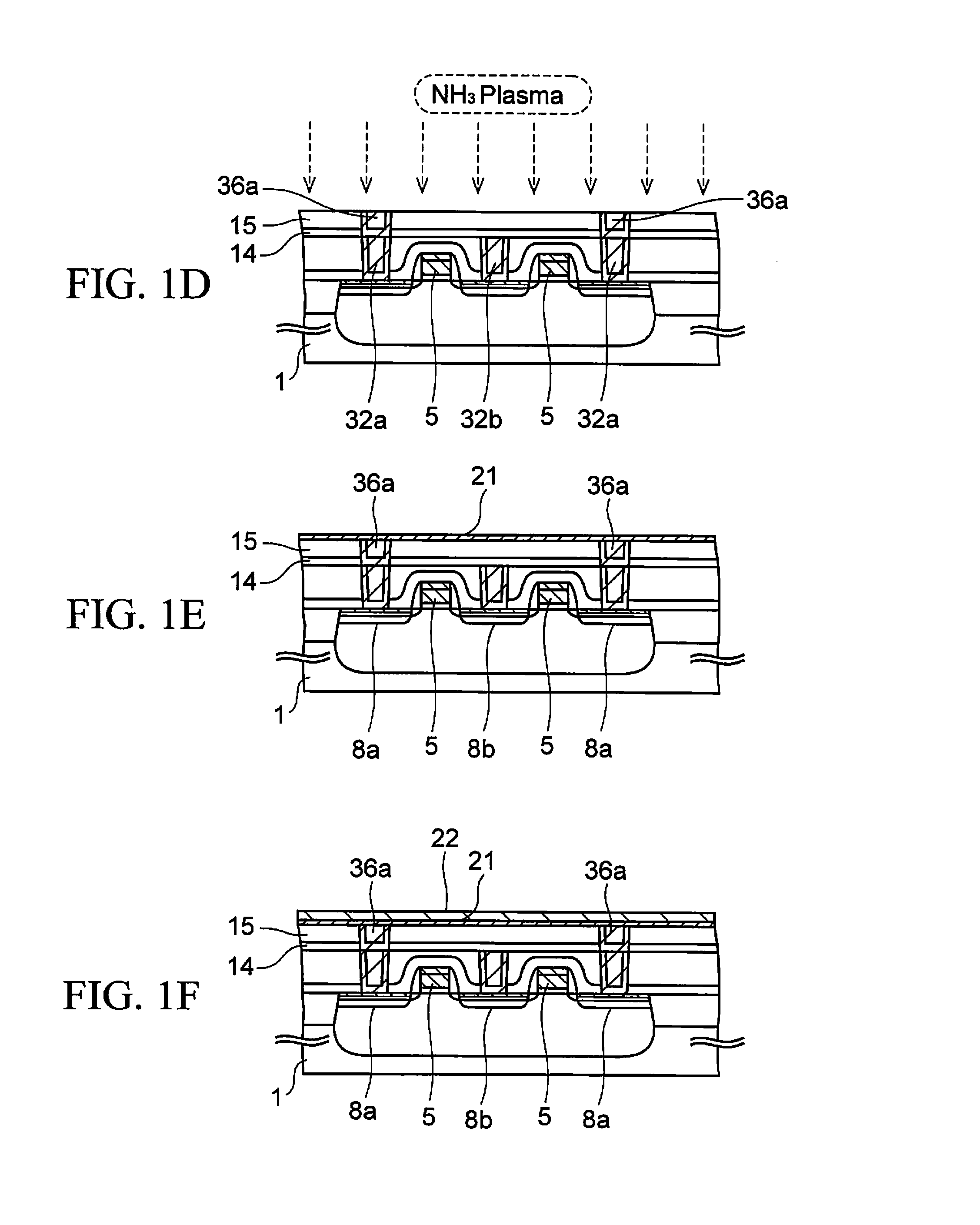
[0223]FIGS. 11A to 11L are cross-sectional views of a semiconductor device according to a second embodiment of the present invention in the process of being manufactured. Incidentally, in these drawings, elements described in the first embodiment are denoted by the same reference numerals as in the first embodiment, and will not be further described below.

[0224]In the step of FIG. 1C of the first embodiment, the third conductive plugs 36a are formed by polishing the glue film 35 and the plug conductive film 36 by CMP.

[0225]However, for the slurry used in the CMP, the polishing speeds of the glue film 35 and the plug conductive film 36 are faster than that of the underlying insulating film 15 thereunder. It is therefore difficult to align the heights of the respective upper surfaces of the third conductive plugs 36a and the underlying insulating film 15 with each other at the time when the CMP is finished.

[0226]Accordingly, as shown in FIG. 11A, recesses 15b are ...

third embodiment

(3) Third Embodiment

[0257]FIG. 12 is a cross-sectional view of a semiconductor device according to a third embodiment.

[0258]The third embodiment differs from the second embodiment in the following point. In the third embodiment, in the CMP step of FIG. 11D, the planarization conductive film 50 is removed from the upper surface of the underlying insulating film 15 to leave the planarization conductive film 50 only in the recesses 15b. The third embodiment and the second embodiment are identical except for the above points.

[0259]Also in the third embodiment, the capacitor dielectric films 24a are formed of the first ferroelectric film 24b and the second ferroelectric film 24c, and the first ferroelectric film 24b is annealed in an atmosphere containing an oxidizing gas, e.g., a mixed atmosphere of oxygen and argon.

[0260]Thus, impurities such as carbon and water in the first ferroelectric film 24b are removed, and it is made possible to simultaneously achieve an increase in the switchi...


PUM

PropertyMeasurementUnit
temperatureaaaaaaaaaa

Abstract

The present invention provides a method of manufacturing a semiconductor device. The method includes the steps of forming a first interlayer insulating film over a silicon substrate; forming a first conductive film on the first interlayer insulating film; forming a first ferroelectric film, which is crystallized, on the first conductive film; annealing the first ferroelectric film; after the annealing, forming, on the first ferroelectric film, a second ferroelectric film made of an amorphous material or a microcrystalline material; forming a second conductive film on the second ferroelectric film; and forming a capacitor by patterning the first and second conductive films and the first and second ferroelectric films.

Description

CROSS-REFERENCE TO RELATED APPLICATIONS[0001]This application is based on and claims priority of Japanese Patent Application No. 2006-182308 filed on Jun. 30, 2006, the entire contents of which are incorporated herein by reference.BACKGROUND OF THE INVENTION[0002]1. Field of the Invention[0003]The present invention relates to a method of manufacturing a semiconductor device.[0004]2. Description of the Related Art[0005]In recent years, with progress of digital technology, nonvolatile memories, in which a large volume of data can be stored at a high speed, have been developed.[0006]As such nonvolatile memories, flush memories and ferroelectric memories are known.[0007]Of these, flush memories have a floating gate buried in a gate insulating film of an insulated-gate field-effect transistor (IGFET), and accumulate, in this floating gate, charge representing information to be stored, thus storing the information. However, in the flash memory, tunnel current needs to be passed through th...

Claims


Application Information

Patent Timeline
Patent Type & Authority Patents(United States)
IPC IPC(8): H01G7/06
CPCH01L21/2855H01L21/32051H01L21/76816H01L21/76826H01L28/56
Inventor WANG, WENSHENGNAKABAYASHI, MASAAKIMATSUURA, KATSUYOSHI
Owner FUJITSU SEMICON LTD
Why Eureka
Try Eureka