

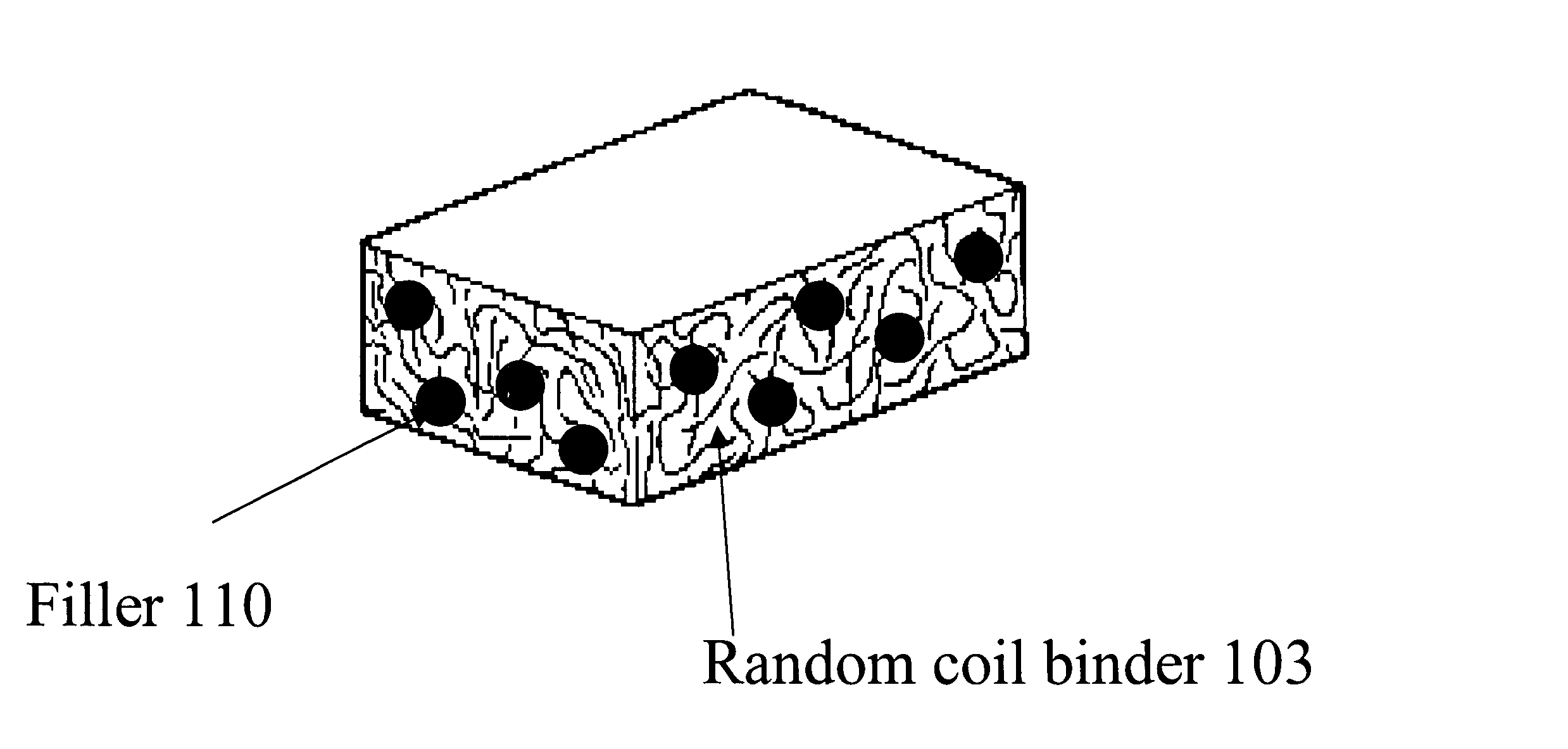
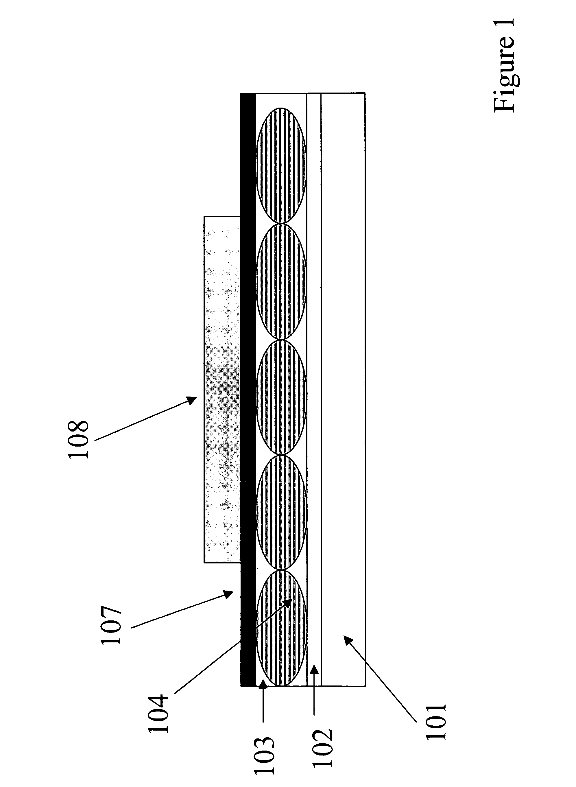
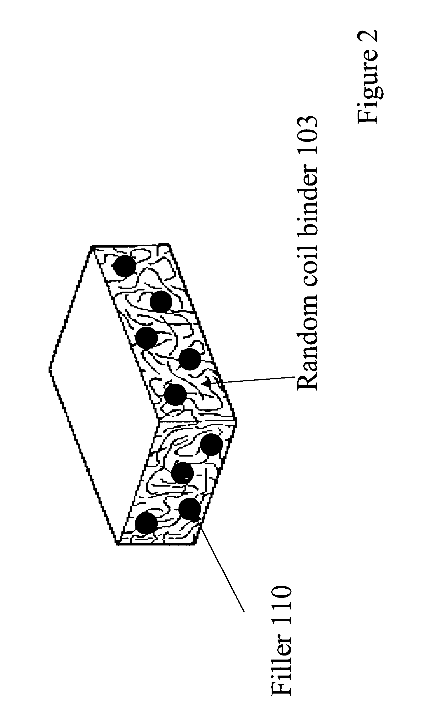
High performance flexible display with improved mechanical properties having electrically modulated material mixed with binder material in a ratio between 6:1 and 0.5:1
a technology of mechanical properties and flexible displays, applied in the direction of materials nanotechnology, instruments, chemistry apparatuses and processes, etc., can solve the problems of loss of performance, uv radiation is harmful to liquid crystals, and the change of the reflected color, so as to achieve low switching voltage, improve the effect of mechanical properties, and reduce the effect of uv radiation
- Summary
- Abstract
- Description
- Claims
- Application Information
AI Technical Summary
Benefits of technology
Problems solved by technology
Method used
Image

Examples
example 1
[0130]This example illustrates the scratch resistance of a coating of display material prepared according to the method of the invention compared to a control coating.
[0131]A chiral nematic liquid crystal (CLC) composition with center wavelengths of reflection (CWR) at 590 nm was prepared by adding the appropriate amount of a high twist chiral dopant to the nematic host mixture BL087 obtained from Merck, Darmstadt, Germany. The CLC composition also contained 0.2% weight / weight (w / w) of the blue absorbing dye Neopen Yellow 057 from BASF Corporation.
[0132]A dispersion of the CLC composition with CWR at 590 nm was prepared as follows. To 248 grams of distilled water was added 3.7 grams of Ludox™ colloidal silica suspension and 7.7 grams of a 10% w / w aqueous solution of a copolymer of methylaminoethanol and adipic acid. To this was added 111 grams of the CLC composition. The mixture was stirred using a Silverson mixer at 5000 rpm. It was then passed through a microfluidizer at 3000 psi....
example 2
[0137]This example illustrates the electro-optic characteristics of a device prepared according to the method of our invention.
[0138]A sample prepared according to method 2 (invention) in Example 1 was kept aside for 48 h to allow the cross-linking of gelatin to go to completion. The coating was then placed on a coating block that was maintained at 30 C. A composition containing 4% Type IV cattle gelatin, 1.4% carbon black and 0.1% Aerosol OT in distilled water was then spread over it using a coating knife with 0.008 cm gap to constitute the protective overcoat. The coating was dried at 30 C. For this top layer or protective overcoat, the temperature of the coating block and the drying temperature were both below the sol-gel transition temperature of the binder. A silver-based conducting ink was then screen printed over the dried protective layer to complete construction of the display device. It was found that a voltage pulse higher than 72 volts switched the display into the refle...
PUM
| Property | Measurement | Unit |
|---|---|---|
| refractive index | aaaaa | aaaaa |
| refractive index | aaaaa | aaaaa |
| particle size | aaaaa | aaaaa |
Abstract
Description
Claims
Application Information