Solar cells
a technology of organic photovoltaic devices and thin films, applied in the field of organic photosensitive optoelectronic devices, can solve the problems of low photovoltaic performance, low external quantum efficiency, and difficult production of efficient crystalline-based devices, and achieve the effect of improving photovoltaic performance and high external quantum efficiency
- Summary
- Abstract
- Description
- Claims
- Application Information
AI Technical Summary
Benefits of technology
Problems solved by technology
Method used
Image

Examples
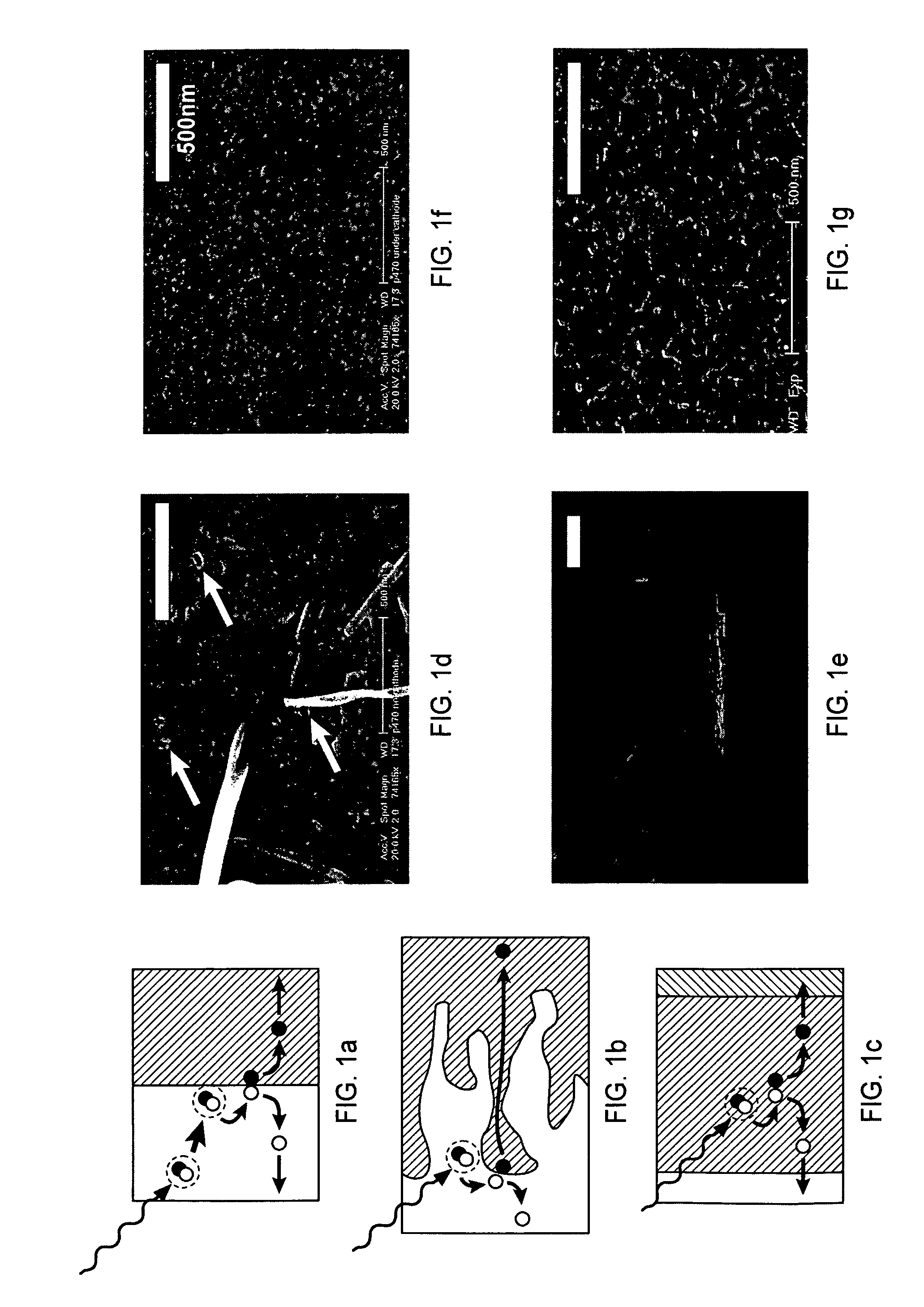
example 1
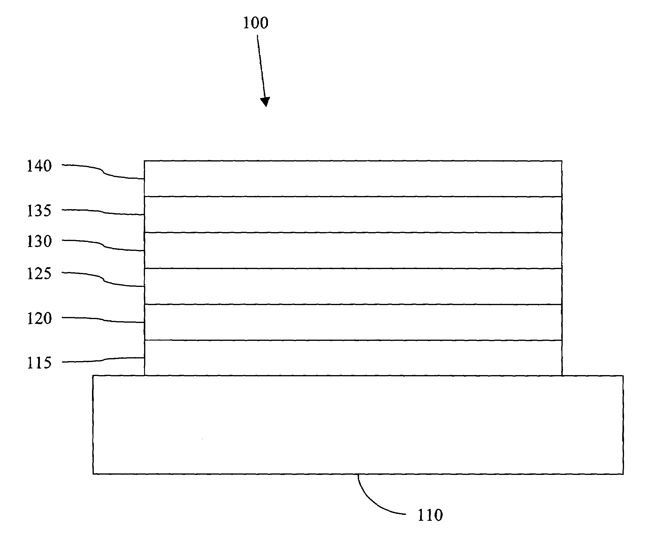
[0096]The PV cells were deposited on glass substrates pre-coated with a 1500 Å thick, transparent, conducting indium-tin-oxide (ITO) anode (sheet resistance 40Ω / □). The substrates were cleaned immediately prior to transferring them into the vacuum system for film deposition. The organic materials were commercially obtained and purified prior to deposition using thermal gradient sublimation. The photoactive materials used were copper phthalocyanine (CuPc) and 3,4,9,10-perylenetetracarboxylic bis-benzimidazole (PTCBI), and bathocuproine (BCP) was used as a contact buffer layer. The organic layers were grown by high vacuum thermal evaporation (base pressure 10−7-10−6 Torr) from a tungsten boat onto a room-temperature substrate. This was followed by the deposition of the metal cathode through a shadow mask, resulting in contact diameters of 0.3 mm and 1 mm.
[0097]After fabrication, the cells were transferred to a vacuum chamber held at 30 m Torr with a heating stage, electrical probes an...
example 2
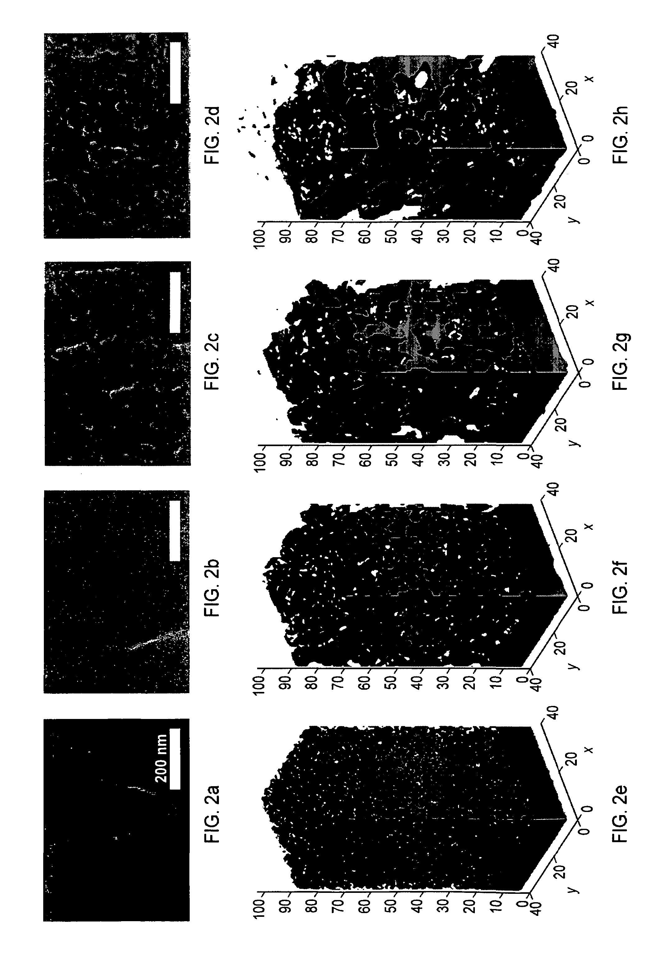
[0100]FIG. 2 contains SEM images of cross-sections of the layer structure: ITO / 5000 Å CuPc:PTCBI (4:1) / 1000 Å Ag are shown for (a) an as-grown film, and for films annealed for 15 min at (b) TA1=450K, (c) TA1=500K, and (d) TA1=550K. The images show phase segregated domains, alternatively rich in CuPc and PTCBI, the cross-sections revealing domains whose size increases with increasing annealing temperature. At 550K, domain sizes of 20 nm are observed.
example 3
[0101]Domain sizes of 20 nm are confirmed by the X-Ray diffraction data shown in FIG. 3. Upon annealing, diffraction peaks corresponding to the orthorhombic α-CuPc phase emerge, and the broad amorphous background signal between 2Θ=2.5° and 12.5° is reduced. The large width of the peaks suggests limited crystalline domain size. For the film annealed at 550K, using the FWHM (full width half maximum) of the peaks at 2Θ=6.7° and 2Θ=12.2°, we calculate a domain size of (12±1) nm, which is consistent with the observations in FIG. 2. This represents a lower limit to the domain size, as the diffraction peaks are also broadened by molecular disorder and large strains associated with the growth of domains within an amorphous matrix. Additional potential contribution to the peak width is residual “doping” of the CuPc and PTCBI-rich phases with PTCBI and CuPc, respectively.
PUM
| Property | Measurement | Unit |
|---|---|---|
| wavelength | aaaaa | aaaaa |
| temperature | aaaaa | aaaaa |
| temperature | aaaaa | aaaaa |
Abstract
Description
Claims
Application Information
 - R&D
- Intellectual Property
- Life Sciences
- Materials
- Tech Scout
- Unparalleled Data Quality
- Higher Quality Content
- 60% Fewer Hallucinations
Browse by: Latest US Patents, China's latest patents, Technical Efficacy Thesaurus, Application Domain, Technology Topic, Popular Technical Reports.
© 2025 PatSnap. All rights reserved.Legal|Privacy policy|Modern Slavery Act Transparency Statement|Sitemap|About US| Contact US: help@patsnap.com