

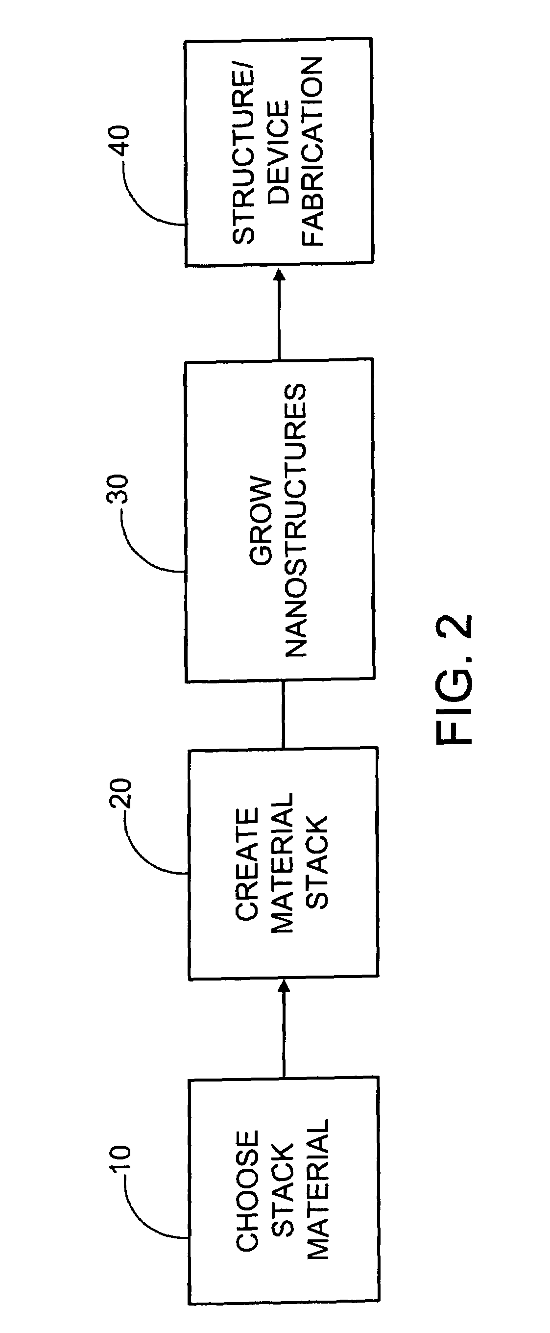
Controlled growth of a nanostructure on a substrate
a nanostructure and controlled growth technology, applied in the field of nanostructures, can solve the problems of inability to achieve perfect control, and increase the cost of new materials
- Summary
- Abstract
- Description
- Claims
- Application Information
AI Technical Summary
Benefits of technology
Problems solved by technology
Method used
Image

Examples
example 1
Electron-Beam Writer
[0189]FIG. 25 shows a SEM image of an embodiment of an electron beam writer that may be used as a nano writer, wherein: DCNT=Diameter of CNT / CNF / nano-structure; LSD=thickness of insulator; LCNT=Length of CNT / CNF / nanostructure; Lg=Distance between CNT / CNF / nanostructure and electrodes; FElas=Elastostatic force acting on CNT / CNF / nanostructure; FElec=Electrostatic force; and FvdW=Van der Waals force. The voltage source in FIG. 25 may be DC or AC source depending on application.
[0190]The structure in FIG. 25 may also be used as an electron beam emitter for use in a display, wherein the position of the nanostructure is controlled while electrons are emitted from the structure onto, for instance, a fluorescent screen that emits photons when excited by electrons, thus providing a visible point. In this way, a display unit (pixel) with localized geometry control (sub pixels) is provided. By forming a plurality of these display units into a system of electron beam emitters...
example 2
Control
[0192]This example presents results that evidence control over the morphology and control over the chemical composition present at the base and the tip of grown carbon nanostructures, see FIGS. 26A and 26B. FIG. 26A is a transmission electron microscopy (TEM) micrograph showing a carbon nanofiber grown on a W metal underlayer. FIG. 26A shows how the morphology can differ based on sample preparation recipe.
[0193]FIG. 26B shows an example of how the chemical composition at the interface (base) and at the tip can be obtained. In FIG. 26B panel (a) there is a TEM image of a grown carbon nanofiber; in panel (b) an EDS spectrum shows the chemical elements at the tip of the fibers (catalyst region); and in panel (c) an EDS spectrum shows the chemical elements at the base of the fibers (underlayer region).
[0194]The CNF grew from a flat catalyst surface and no significant catalyst film break up was observed (see, e.g., Kabir, M. S.; Morjan, R. E.; Nerushev, O. A.; Lundgren, P.; Bengts...
example 3
Incorporating Nanostructures into a CMOS Device
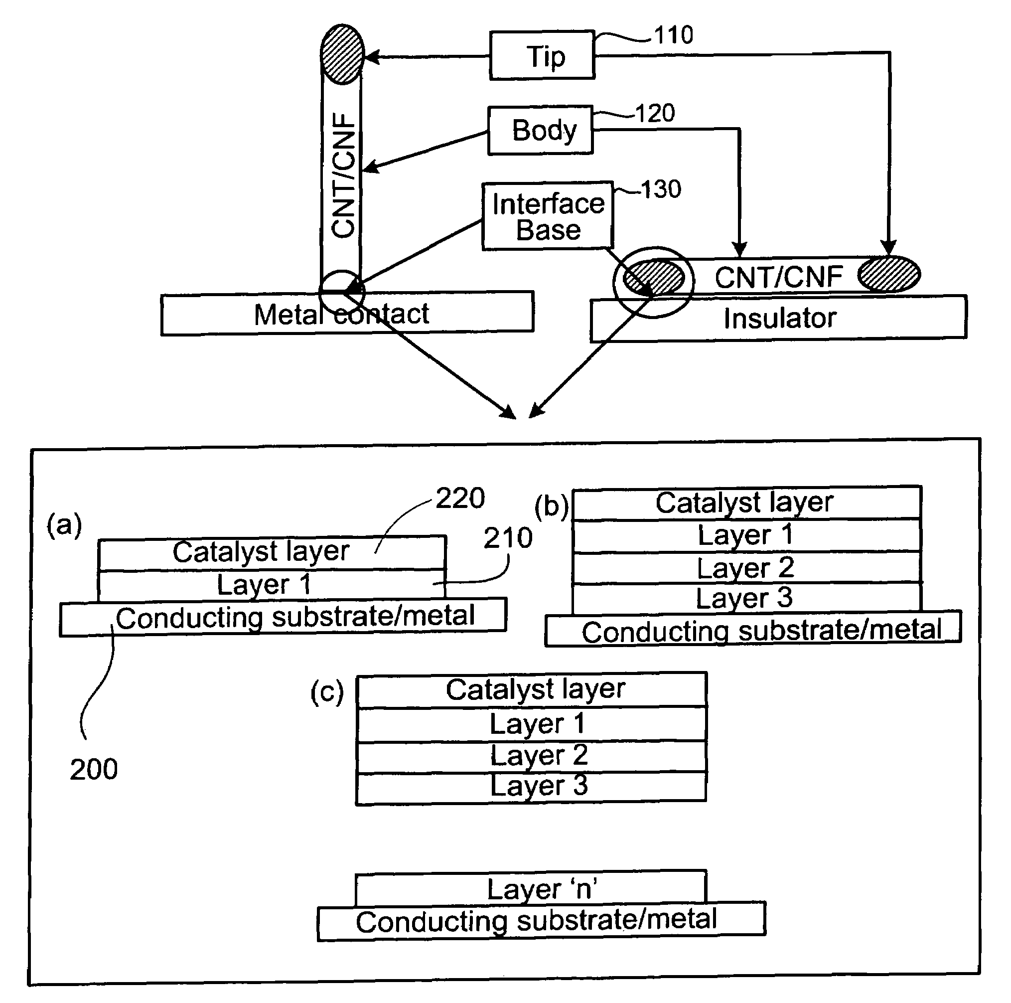
[0195]Nanostructures as described herein can be incorporated into a CMOS device as vertical interconnects. To accomplish this, a filler layer such as an insulator is deposited over a substrate and the nanostructures situated thereon, and then polished / etched back until the nanostructure is exposed at the top. The catalyst layer can be removed, e.g., by etching, once the nanostructure is grown if required.
PUM
| Property | Measurement | Unit |
|---|---|---|
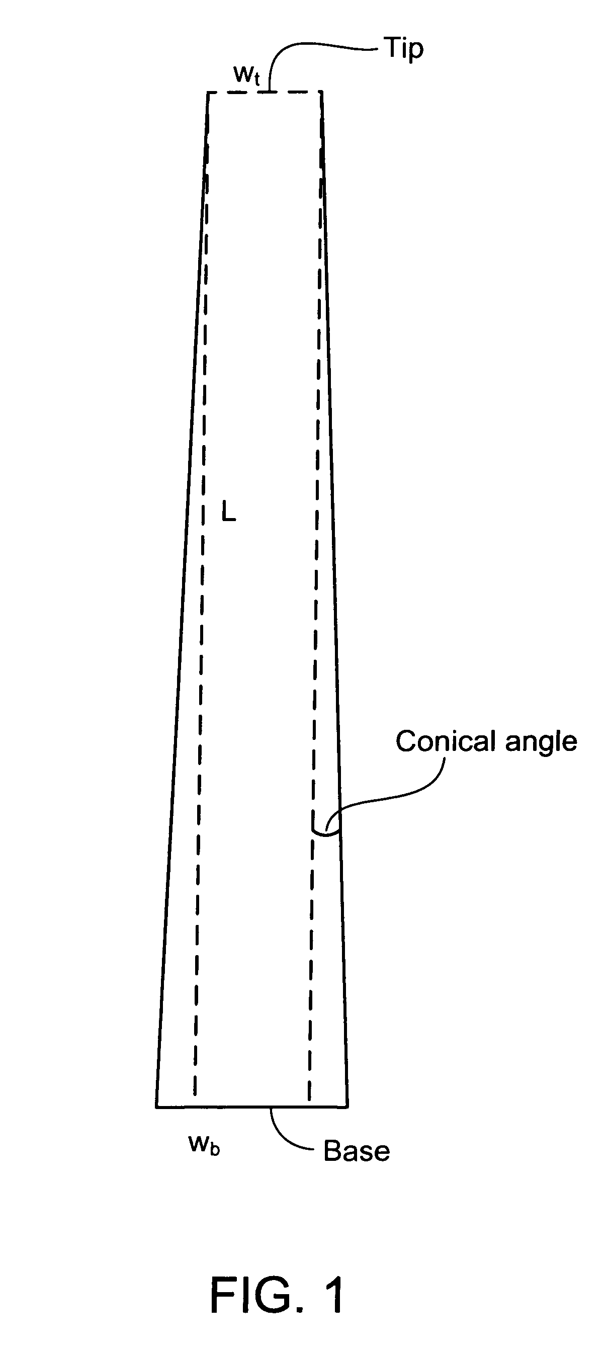
| conical angle | aaaaa | aaaaa |
| thick | aaaaa | aaaaa |
| thick | aaaaa | aaaaa |
Abstract
Description
Claims
Application Information