

Plasma processing method and computer storage medium
a processing method and computer technology, applied in the direction of solid-state diffusion coating, coating, electric discharge tube, etc., can solve the problems of increasing leakage current, reducing operating speed, and conventionally difficult to improve both static characteristics (gate leakage current, source-drain current) and nbti resistance of transistors, so as to improve the quality of oxynitride films, reduce leakage current, and reduce damage at the time of plasma nitridation
- Summary
- Abstract
- Description
- Claims
- Application Information
AI Technical Summary
Benefits of technology
Problems solved by technology
Method used
Image

Examples
Embodiment Construction
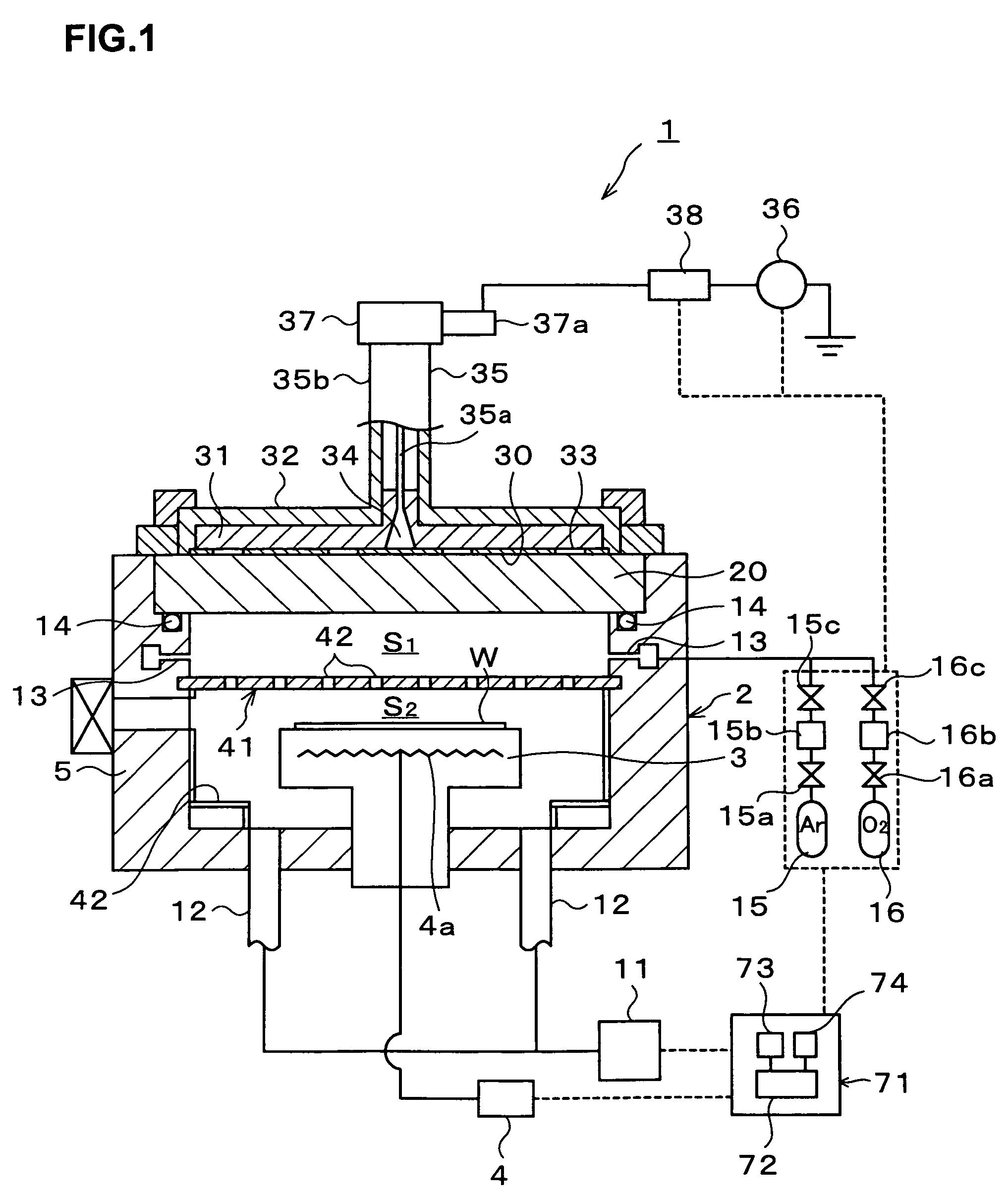
[0029]Hereinafter, an embodiment of the present invention will be described. FIG. 1 shows a state of a vertical cross section of a plasma processing apparatus 1 for carrying out a plasma processing method according to this embodiment, and this plasma processing apparatus 1 includes a process vessel 2 made of, for example, aluminum and having a bottomed cylindrical shape with an upper part being open. The process vessel 2 is grounded. On a bottom of the process vessel 2, provided is a susceptor 3 as a mounting table on which a substrate, for example, a semiconductor wafer (hereinafter, referred to as a wafer) W is mounted. The susceptor 3 is made of a ceramic member of, for example, aluminum nitride, and has therein a heater 4a that generates heat when supplied with power from an external power source 4. This enables heating of the wafer W on the susceptor 3 to a predetermined temperature.
[0030]In the bottom of the process vessel 2, provided are exhaust pipes 12 through which an atmo...
PUM
| Property | Measurement | Unit |
|---|---|---|
| time | aaaaa | aaaaa |
| pressure | aaaaa | aaaaa |
| temperature | aaaaa | aaaaa |
Abstract
Description
Claims
Application Information