Semiconductor chip assembly with welded metal pillar and enlarged plated contact terminal
- Summary
- Abstract
- Description
- Claims
- Application Information
AI Technical Summary
Benefits of technology
Problems solved by technology
Method used
Image

Examples
Embodiment Construction
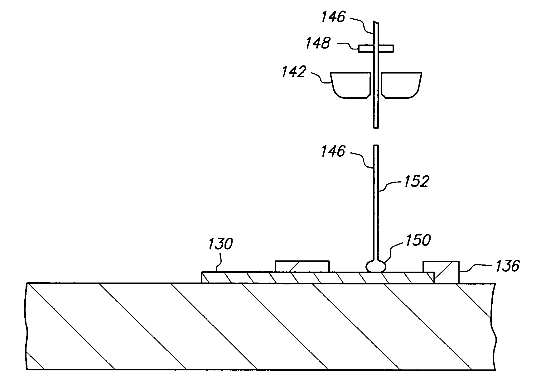
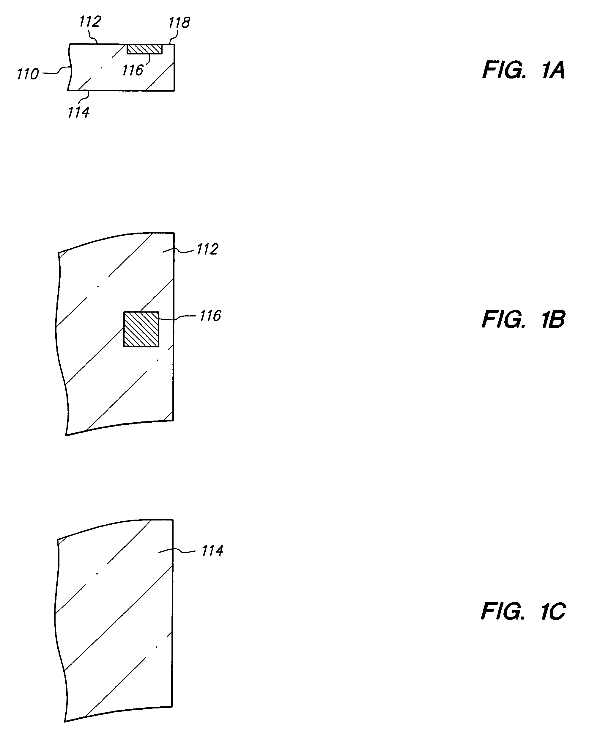
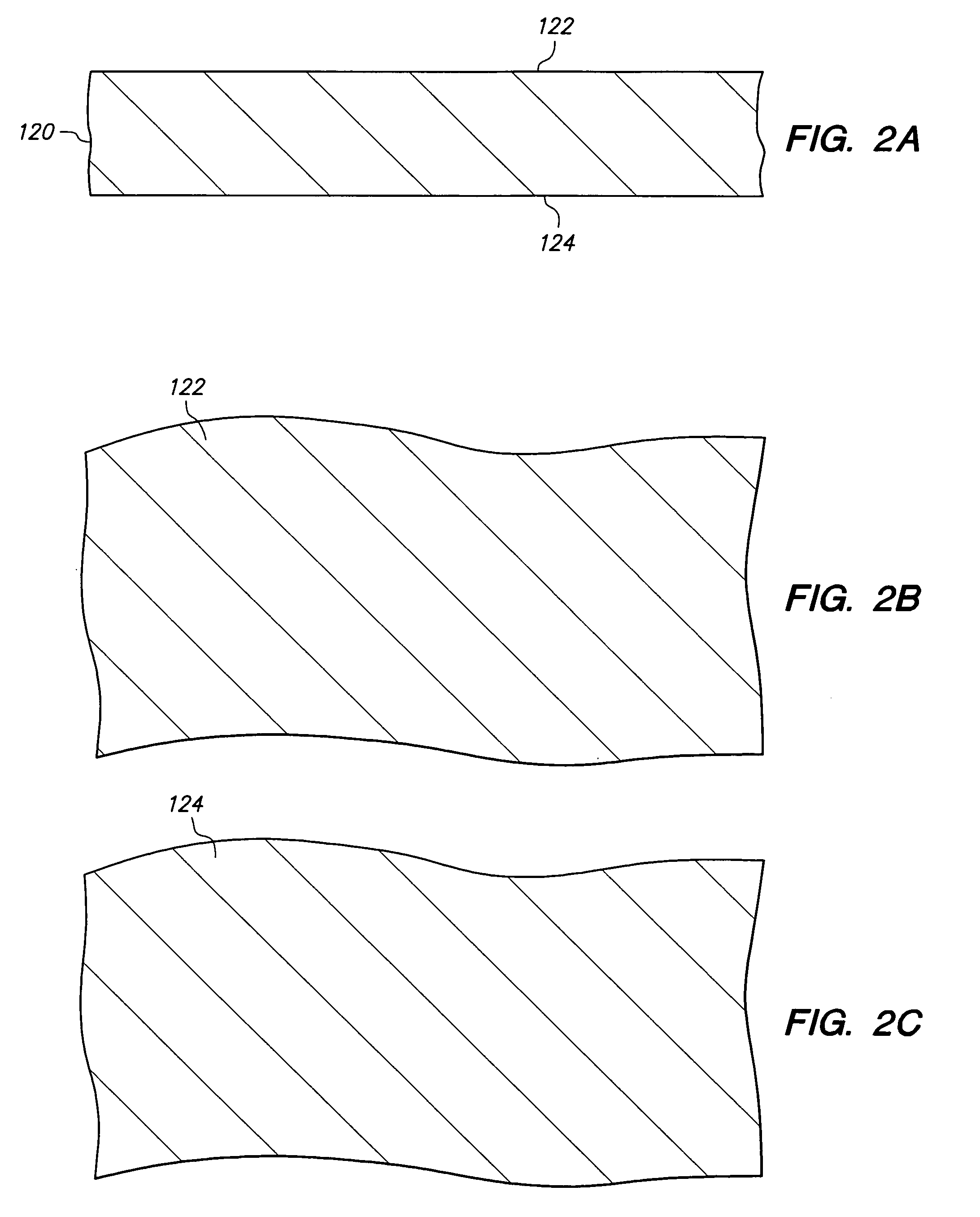
[0086]FIGS. 1A-19A, 1B-19B and 1C-19C are cross-sectional, top and bottom views, respectively, of a method of making a semiconductor chip assembly in accordance with a first embodiment of the present invention.
[0087]FIGS. 1A, 1B and 1C are cross-sectional, top and bottom views, respectively, of semiconductor chip 110 which is an integrated circuit in which various transistors, circuits, interconnect lines and the like are formed (not shown). Chip 110 includes opposing major surfaces 112 and 114 and has a thickness (between surfaces 112 and 114) of 150 microns. Surface 112 is the active surface and includes conductive pad 116 and passivation layer 118.
[0088]Pad 116 is substantially aligned with passivation layer 118 so that surface 112 is essentially flat. Alternatively, if desired, pad 116 can extend above or be recessed below passivation layer 118. Pad 116 provides a bonding site to electrically couple chip 110 with external circuitry. Thus, pad 116 can be an input / output pad or a ...
PUM
 Abstract
Description
Claims
Application Information
PatSnap Eureka turns technology decisions into work you can execute. Powered by our Innovation Knowledge Graph, it runs expert workflows across engineering, life sciences, materials and intellectual property. Get your review-ready output in minutes.


