

Semiconductor device
a technology of semiconductor devices and integrated circuits, applied in semiconductor devices, digital storage, instruments, etc., can solve the problems of difficult high-speed operation in nature, and achieve the effects of low power consumption, low charging current of data lines, and no nois
- Summary
- Abstract
- Description
- Claims
- Application Information
AI Technical Summary
Benefits of technology
Problems solved by technology
Method used
Image

Examples
first embodiment
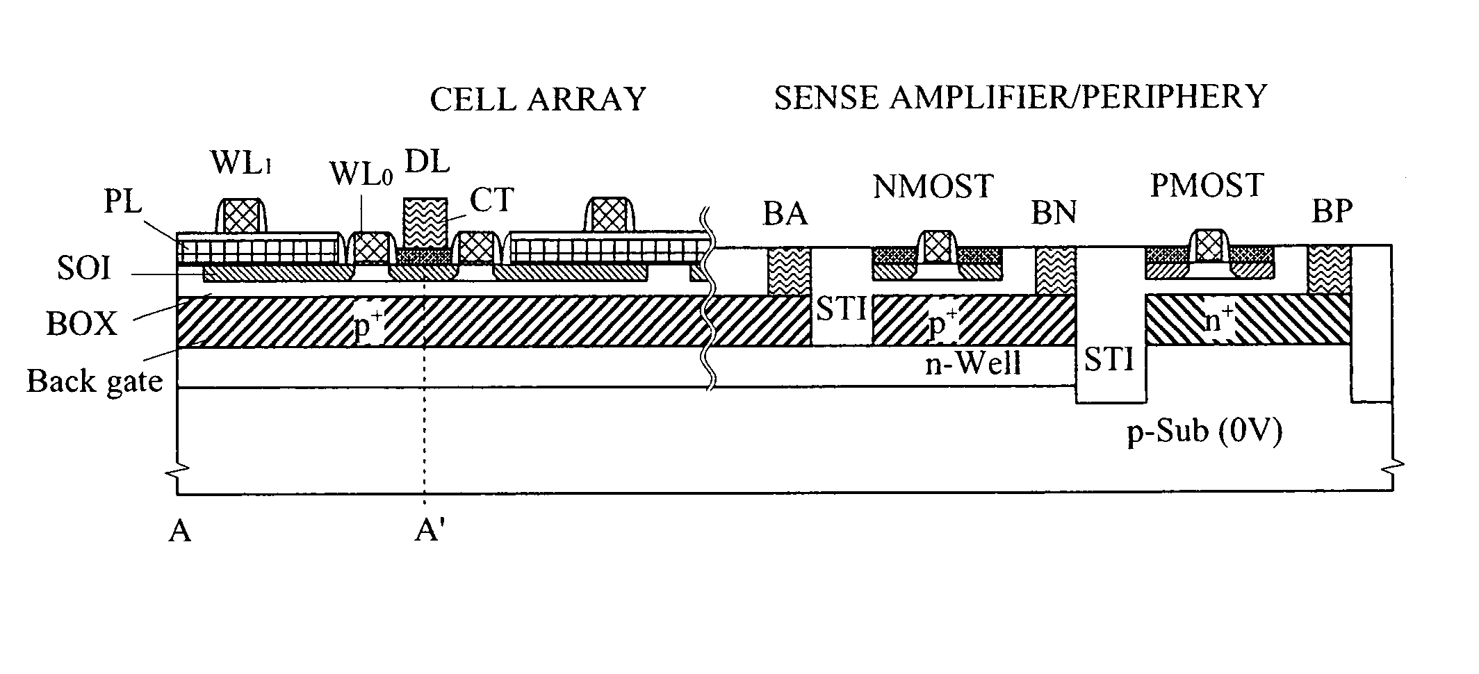
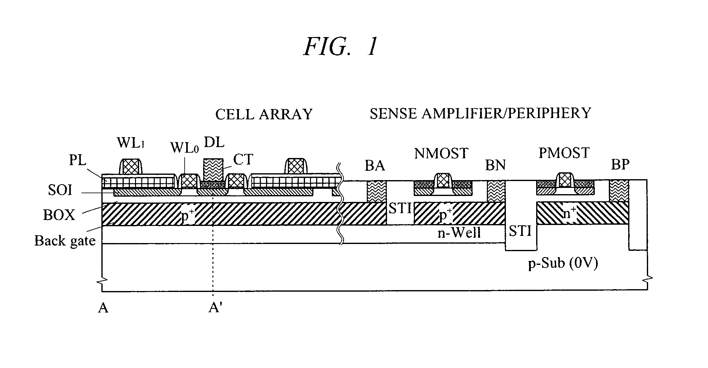
[0035]FIG. 1 is a sectional view of a DRAM using the SOI MOST according to an embodiment of the present invention. In this structure, since superfluous impurities are not diffused in a storage node of the memory cell, the leakage current is low enough to be ignorable. Accordingly, the data retention characteristics are improved, for example, the refresh time is sufficiently increased. Also, even when the alpha ray and the cosmic ray are entered, since the collection area in the cell is extremely small, the soft error can be reduced to an ignorable level. Further, since the variation in VT is significantly reduced, the offset voltage of the sense amplifier is lowered and the sensitivity thereof is improved. Furthermore, although the word voltage has to be boosted to VDD+VT or more in order to fully write the high voltage (VDD) from the data line to the sell node in a DRAM, this boosting voltage can be reduced owing to the small variation in VT, and since there is no body bias effect,...
second embodiment
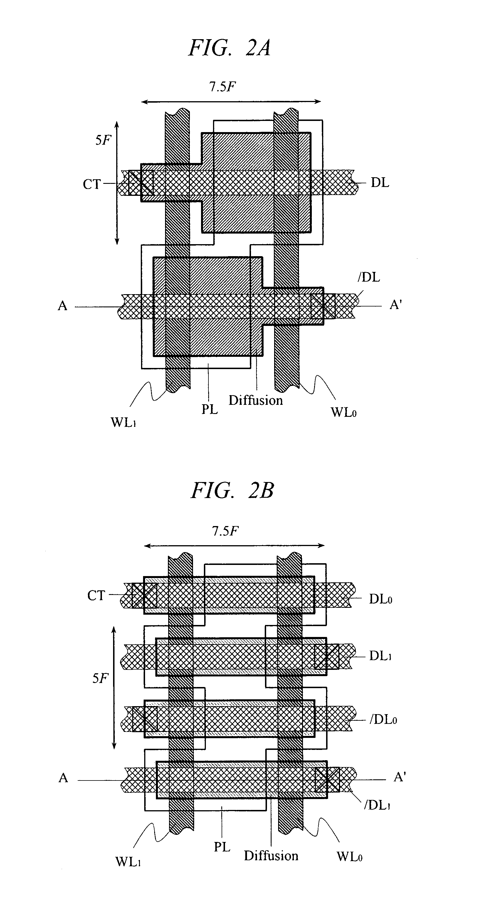
[0037]FIG. 2 shows two types of cells laid out based on the feature size F, and FIG. 3 shows a data line circuit corresponding to them. Although this is the low-noise and high-integrated cell layout even if the SOI MOST is not used, since the remarkable advantages as described above can be obtained in the SOI structure, the description will be made on the assumption that the SOI structure is formed in the cross section. Note that the cross section of the cell shown in FIG. 1 corresponds to the cross section taken along the A-A′ line of these cells. FIG. 3A shows the cell (hereinafter, abbreviated to 1-T cell) connected to one of two intersections between the word line WL and the paired data lines (DL and / DL), and one cell processes one bit of information. The case where the cell connected to DL is read will be considered here. When the stored voltage is VDD, the signal voltage vS determined by the difference between VDD and the precharge voltage VDD / 2 of the data line, the capacita...
third embodiment
[0042]FIG. 7 shows an embodiment in which a gate and a well (terminal BN in FIG. 1) of each MOST of a sense amplifier are connected, and VT of each MOST is dynamically changed to operate the sense amplifier at high speed. Regardless of the 1-T cell and the 2-T cell, even the totally new enhancement / depletion type sense amplifier capable of the dynamic operation can be realized. This is obvious from the example of the NMOST of FIG. 9C and VDD=1 V. Since both the gate voltage and the well voltage of M1 and M2 are VDD / 2 (0.5 V) at the end of the precharging, VT thereof is 0.05 V (point A). When the negative signal vS is read to the data line DL0 and the amplification thereof is started, the sense amplifier activation signal ACT is turned on, and M1 in the NMOS amplifier first starts to be turned on and the gate voltage of M2 starts to decrease. At this time, since vS is small, M2 is slightly turned on to decrease the gate voltage of M1. However, due to the voltage difference of vS, it ...
PUM
 Abstract
Description
Claims
Application Information