Encapsulated devices and method of making

a technology of encapsulation and devices, applied in the field of encapsulation devices, can solve the problems of device degradation, device damage, and permeation of environmental gases, and achieve the effects of reducing the number of ester moieties, reducing the number of polar regions, and high packing density

Active Publication Date: 2010-08-03
SAMSUNG DISPLAY CO LTD
View PDF455 Cites 41 Cited by
  • Summary
  • Abstract
  • Description
  • Claims
  • Application Information

AI Technical Summary

Benefits of technology

[0023]The present invention meets this need by providing a method of encapsulating an environmentally sensitive device. The method includes providing a substrate; placing at least one environmentally sensitive device adjacent to the substrate; and depositing at least one barrier stack adjacent to the environmentally sensitive device, the at least one barrier stack comprising at least one barrier layer and at least one polymeric decoupling layer, wherein the at least one polymeric decoupling layer is made from at least one polymer precursor, and wherein the polymeric decoupling layer has at least one of: a reduced number of polar regions; a high packing density; a reduced number of regions that have bond energies weaker than a C—C covalent bond; a reduced number of ester moieties; increased Mw of the at least one polymer precursor; increased chain length of the at least one polymer precursor; or reduced conversion of C═C bonds.

Problems solved by technology

Many devices are subject to degradation caused by permeation of environmental gases or liquids, such as oxygen and water vapor in the atmosphere or chemicals used in the processing of the electronic product.
We have found that some of the devices being encapsulated have been damaged by the plasma used in depositing the barrier and / or decoupling layers.
Plasma damage has occurred when a substrate with an environmentally sensitive device on it, such as an OLED, is encapsulated with a multi-layer barrier stack in which a plasma based and / or assisted process is used to deposit a barrier layer or decoupling layer.
For example, plasma damage has occurred when reactively sputtering a barrier layer of AlOx under conditions suitable for achieving barrier properties, sputtering a barrier layer of AlOx onto the top surface of an environmentally sensitive device, and / or sputtering a barrier layer of AlOx on a vacuum deposited, acrylate based polymeric layer.
Plasma damage involves a negative impact on the electrical and / or luminescent characteristics of a device resulting from encapsulation.
It is important to note that plasma damage is dependent on the design of the device to be encapsulated.
According to Treger, this phenomenon significantly reduces the usefulness of the composite as a moisture barrier, since the defects often propagate through all of the inorganic layers if no organic layer is interposed between them.
However, the cost of the moisture barrier increases with each layer that is deposited.
Also, if the layers are too thin, there will be voids of incomplete coverage in the layers, and this will increase the permeability of the composite.
However, they indicate that the range of improvement that is possible with the polymer layer may be insignificant relative to the improvement of the inorganic layer because the effective diffusion of the inorganic layer is at least four orders of magnitude lower than that of the polymer layers.
On the other hand, it is known that in some cases plasma and / or radiation exposure degrades the functional properties of polymers.

Method used


Image

  • Encapsulated devices and method of making
  • Encapsulated devices and method of making
  • Encapsulated devices and method of making

Examples


example 1

[0068]Polymer films were made using different blends of acrylate monomers. The formulations are shown in Table 1. Polymer layers made using tripropyleneglycol diacrylate have been described in, for example, “Plasma treatment of PET and acrylic coating surfaces-I. In-situ XPS measurements,” Shi, et al., J. Adhesion Sci. Technol., Vol. 14, No. 12, pp 1485-1498 (2000), which is incorporated herein by reference. Formulation 1, which incorporates tripropyleneglycol diacrylate, has been used as a basis for comparison for the other formulations.

[0069]

TABLE 1Component Wt %Component1234567Methoxy Tripropyleneglycol Acrylate3.5Lauryl Acrylate17.423.222.2Hexanediol Diacrylate (HDODA)65.162.219.5Tripropyleneglycol Diacrylate (TPGDA)69.6Dodecanediol Dimethacrylate73.5Propoxylated Hexanediol Diacrylate93.0Trimethylolpropane Triacrylate (TMPTA)8.010.6Triethoxy Trimethylolpropane Triacrylate14.5Esterdiol diacrylate99Polyfunctional Adhesion Promoter19.8Polybutadiene Dimethacrylate79.4Photoinitiator ...

example 2

[0079]The change in transmission of Ca coupons on glass substrates encapsulated with a multilayer barrier is a good vehicle to test the effectiveness of barrier structures. In the examples shown in FIG. 6A-C the multilayer structure was constituted by an oxide layer 100 nm thick and 6 polymer / oxide pairs [polymer (0.5 μm) / oxide (40 nm)]. Encapsulated Ca coupons were aged for 400 hr at 60° C. and 90% RH. FIG. 6A shows that formulation 4 (5.5×10²⁰ n / ml of ether linkages) has no increased transmission, and thus, no barrier failure. FIG. 6B shows that formulation 1 (3.6×10²¹ n / ml of ether linkages) has increased transmission at the edges of the calcium area. In FIG. 6C, the entire calcium area is fading, indicating extreme barrier failure for formulation 5 (3.2×10²¹ n / ml of ether linkages). FIG. 6D shows a Ca coupon with a multilayer structure constituted by an oxide layer 100 nm thick and only 3 polymer / oxide pairs (polymer (0.7 μm) / oxide (40 nm)). The polymer layer was made with Formu...

example 3

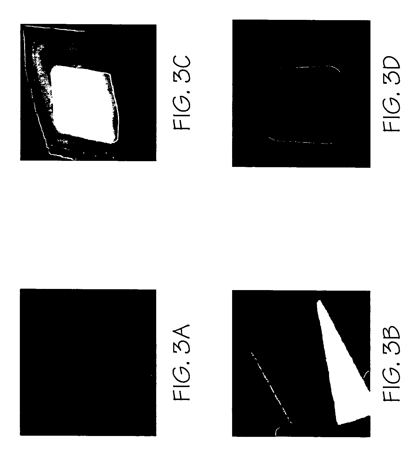
[0084]Barrier stacks were formed on OLED test pixels using various polymer formulations. The samples were stored for 500 hr and tested in a dry box to avoid exposure to moisture. Differences were visually observed within 24 hr.

[0085]FIG. 9A shows formulation 1 (3.6×10²¹ n / ml of ether linkages; 4.7—Ohnishi parameter) after coating, and FIG. 9B shows the appearance of black spots after storage. FIG. 9C shows formulation 4 (5.×1020 of ether linkages; 4.2—Ohnishi parameter) after coating, while FIG. 9D shows that no black spots appeared after storage.

[0086]Polymeric decoupling layers can be formed from blends of one or more reactive precursors. These will have one or more reactive groups per unit (molecule) that undergo a linking / cross-linking reaction. The reactive groups born by all members of the blend may be the same (e.g., acrylic, methacrylic and vinyl), which self react and / or undergo addition reactions to form chains (e.g. polymethylmethacrylate or polyvinyl acetate). A distinct...


PUM


Abstract

A method of encapsulating an environmentally sensitive device. The method includes providing a substrate; placing at least one environmentally sensitive device adjacent to the substrate; and depositing at least one barrier stack adjacent to the environmentally sensitive device, the at least one barrier stack comprising at least one barrier layer and at least one polymeric decoupling layer, wherein the at least one polymeric decoupling layer is made from at least one polymer precursor, and wherein the polymeric decoupling layer has at least one of: a reduced number of polar regions; a high packing density; a reduced number of regions that have bond energies weaker than a C—C covalent bond; a reduced number of ester moieties; increased Mw of the at least one polymer precursor; increased chain length of the at least one polymer precursor; or reduced conversion of C═C bonds. An encapsulated environmentally sensitive device is also described.

Description

[0001]This application claims the benefit of U.S. Provisional Application Ser. No. 60 / 711,136, filed Aug. 25, 2005, entitled “Encapsulated Devices and Method of Making.”BACKGROUND OF THE INVENTION[0002]The present invention relates generally to encapsulated devices, and more particularly to barriers for encapsulation, and to methods for making layers for said barriers.[0003]Many devices are subject to degradation caused by permeation of environmental gases or liquids, such as oxygen and water vapor in the atmosphere or chemicals used in the processing of the electronic product. Some devices are often encapsulated in order to prevent degradation.[0004]Various types of encapsulated devices are known. For example, U.S. Pat. No. 6,268,695, entitled “Environmental Barrier Material For Organic Light Emitting Device And Method Of Making,” issued Jul. 31, 2001; U.S. Pat. No. 6,522,067, entitled “Environmental Barrier Material For Organic Light Emitting Device And Method Of Making,” issued F...

Claims


Application Information

Patent Timeline
Patent Type & Authority Patents(United States)
IPC IPC(8): H01L21/00
CPCH01L51/448H01L51/5256Y02E10/549H10K30/88H10K50/8445H10K50/84
Inventor MORO, LORENZAKRAJEWSKI, TODD L.
Owner SAMSUNG DISPLAY CO LTD
Why Eureka
Try Eureka