Use of ultra-high magnetic fields in resputter and plasma etching

a plasma etching and ultra-high magnetic field technology, applied in electrical discharge tubes, decorative arts, electrical apparatus, etc., can solve the problems of not having enough energy to damage the dielectric layer, low energy ions, etc., and achieve the effect of reducing the roughness of the dielectric surface, reducing the incorporation of sputtering ions, and improving the adhesion of subsequently deposited layers

Active Publication Date: 2011-03-01
NOVELLUS SYSTEMS
View PDF199 Cites 24 Cited by
  • Summary
  • Abstract
  • Description
  • Claims
  • Application Information

AI Technical Summary

Benefits of technology

[0006]Advantageously, in some embodiments, the wafer encounters a high flux of low energy ions, which do not have sufficient energy to damage the dielectric layer. Specifically, microtrenching of the dielectric layer and incorporation of sputtering ions into the dielectric can be substantially minimized, and, in some cases, avoided. Dielectric surface roughening can also be reduced. The reduction in dielectric damage results in improved adhesion of subsequently deposited layers, and, consequently, in improved reliability of the formed IC devices. Further, elimination of microtrenching results in reduced line-to-line leakage due to elimination of regions of excessively high current density. Microtrenching can be avoided by using an ion flux having low ion energy, such as a flux having an ion energy of less than about 250 eV at the exposed wafer surface. In some embodiments, provided

Problems solved by technology

Advantageously, in some embodiments, the wafer encounters a high flux of low e

Method used


Image

  • Use of ultra-high magnetic fields in resputter and plasma etching
  • Use of ultra-high magnetic fields in resputter and plasma etching
  • Use of ultra-high magnetic fields in resputter and plasma etching

Examples


Embodiment Construction

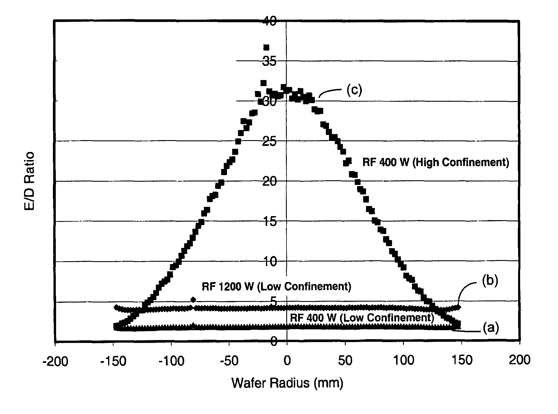
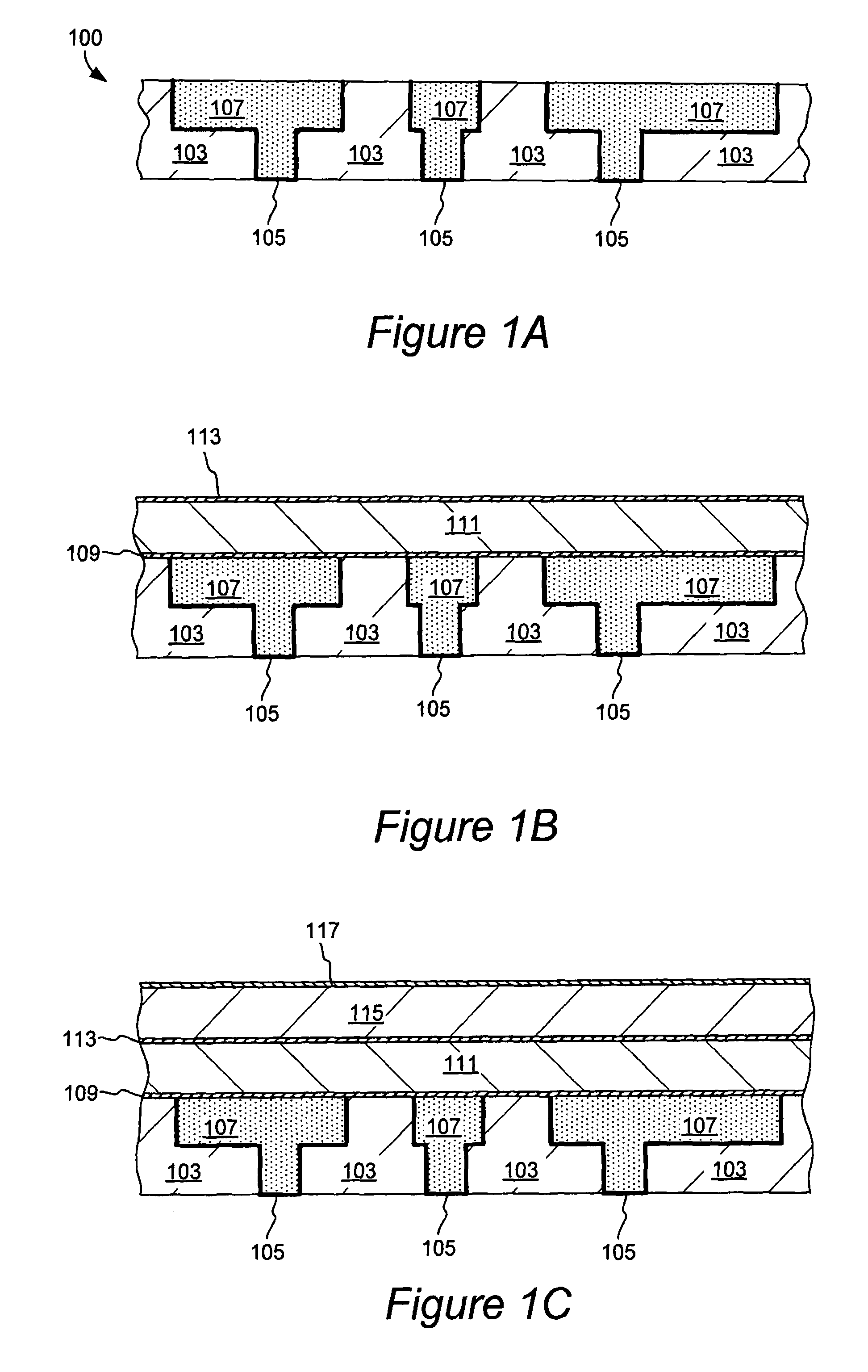
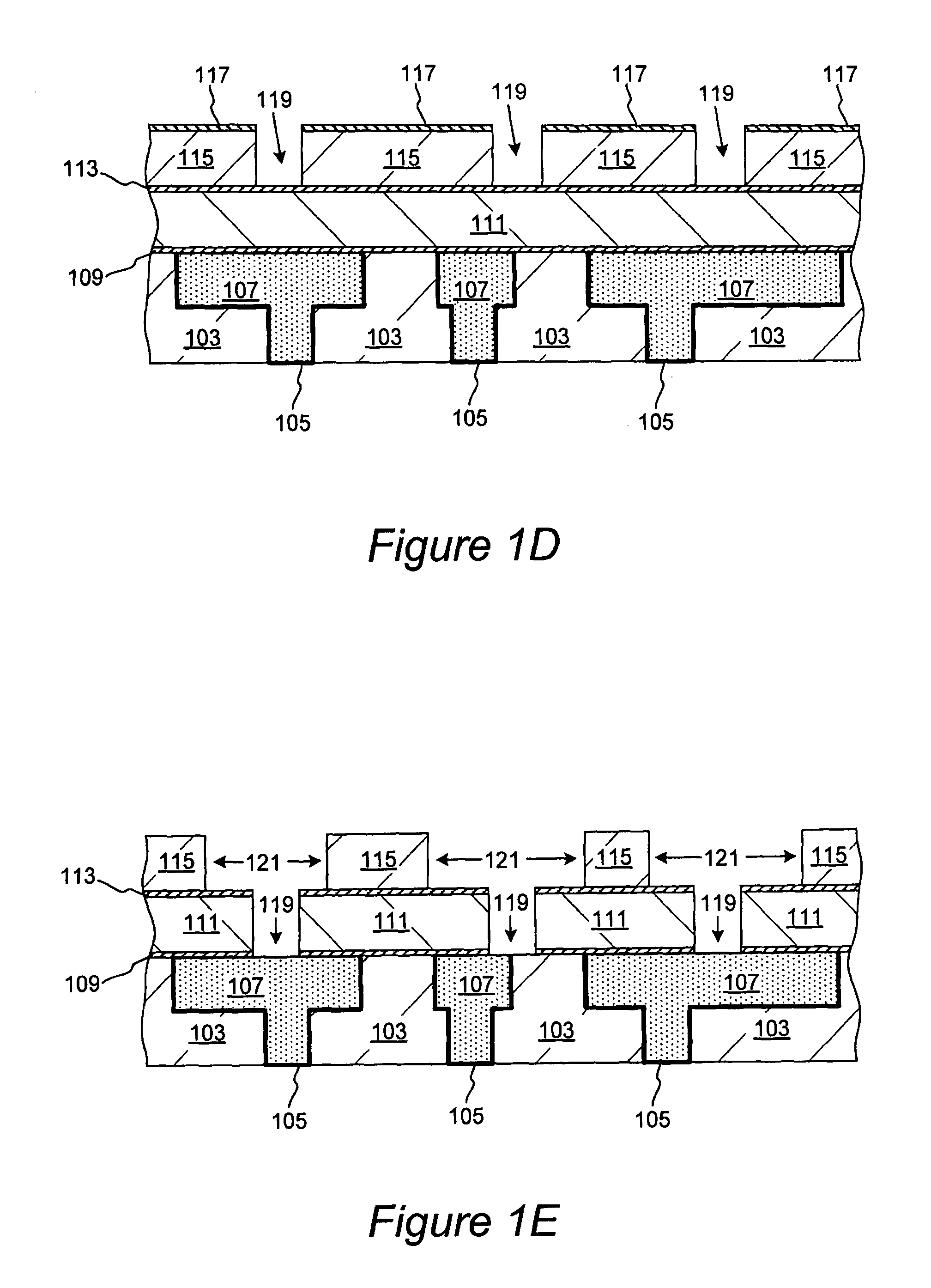
[0036]Methods for generating high density plasmas in PVD and plasma pre-clean reactors are herein provided. According to one aspect, these plasmas can be generated by forming an ultra-high density plasma (e.g., a plasma having a plasma density of at least about 1013 electrons / cm3) in a high confinement regime effected by an ultra-high magnetic field (e.g., a field having a strength of at least about 1 Tesla). These methods can be used in a variety of IC fabrication processes, such as in plasma etching and resputtering. For example, these methods can be used for resputtering diffusion barrier and seed layer materials in Damascene processing. Plasma etching and resputtering will be used interchangeably throughout this document and refer to plasma-based methods in which net material removal is achieved at least at one position on the wafer (e.g., at the via bottom, or at the bottom of the recessed feature being resputtered).

[0037]While these methods will be primarily illustrated in the...


PUM

PropertyMeasurementUnit
Fractionaaaaaaaaaa
Fractionaaaaaaaaaa
Poweraaaaaaaaaa

Abstract

Methods for resputtering and plasma etching include an operation of generating an ultra-high density plasma using an ultra-high magnetic field. For example, a plasma density of at least about 1013 electrons/cm3 is achieved by confining a plasma using a magnetic field of at least about 1 Tesla. The ultra-high density plasma is used to create a high flux of low energy ions at the wafer surface. The formed high density low energy plasma can be used to sputter etch a diffusion barrier or a seed layer material in the presence of an exposed low-k dielectric layer. For example, a diffusion barrier material can be etched with a high etch rate to deposition rate (E/D) ratio (e.g., with E/D>2) without substantially damaging an exposed dielectric layer. Resputtering and plasma etching can be performed, for example, in iPVD and in plasma pre-clean tools, equipped with magnets configured for confining a plasma.

Description

FIELD OF THE INVENTION[0001]The present invention pertains to methods of resputtering layers of material on a partially fabricated integrated circuit. The methods are particularly useful for sputter etching diffusion barrier layers and copper seed layers. The methods can also be applied for sputter etch back of other wafer materials, such as conductive lines.BACKGROUND OF THE INVENTION[0002]Miniaturization of integrated circuit (IC) devices demands superior electrical properties from both dielectric and conductive materials used in the manufacturing of an integrated circuit. Dielectric materials with low dielectric constant (low-k and ultra low-k dielectrics) have replaced the traditionally used silicon dioxide as an inter-layer dielectric (ILD) material, while copper has replaced aluminum as a conducting material in many applications due to its lower resistivity. The low-k dielectric materials used in the IC device processing include carbon doped silicon dioxide, hydrogenated silic...

Claims


Application Information

Patent Timeline
IPC IPC(8): H01L21/302
CPCH01J37/321H01J37/3402H01L21/2855H01L21/32131H01L21/76805H01L21/76844H01L21/76865H01L21/76873
Inventor KINDER, RONALD L.PRADHAN, ANSHU A.
Owner NOVELLUS SYSTEMS
Why Eureka
Try Eureka