

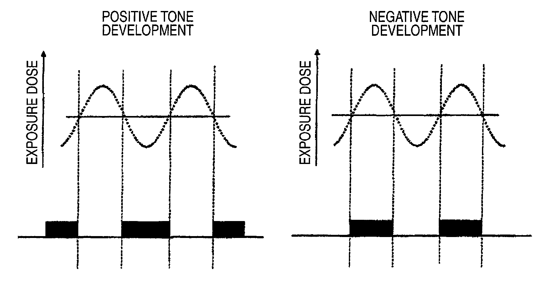
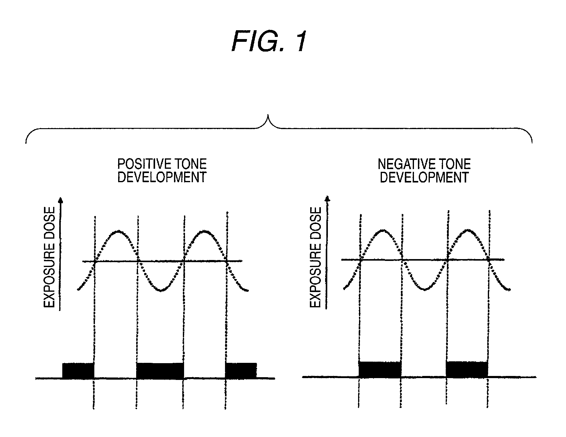
Pattern forming method
a technology of pattern and forming method, which is applied in the field of pattern forming method, can solve the problems of deterioration of resolution, difficulty in finding an appropriate combination of resist composition, and developer, and achieve the effect of improving the exposure latitud
- Summary
- Abstract
- Description
- Claims
- Application Information
AI Technical Summary
Benefits of technology
Problems solved by technology
Method used
Image

Examples
synthesis example 1
Synthesis of Resin (A1)
[0658]Under a nitrogen stream, 20 g of a 6 / 4 (by mass) mixed solvent of propylene glycol monomethyl ether acetate and propylene glycol monomethyl ether was charged into a three-neck flask and heated at 80° C. (Solvent 1). Also, γ-butyrolactone methacrylate, hydroxyadamantane methacrylate and 2-methyl-2-adamantyl methacrylate were dissolved in a molar ratio of 40 / 30 / 30 in a 6 / 4 (by mass) mixed solvent of propylene glycol monomethyl ether acetate and propylene glycol monomethyl ether to prepare a 22 mass % monomer solution (200 g). Thereto, an initiator V-601 (produced by Wako Pure Chemical Industries, Ltd.) was added and dissolved in an amount of 8 mol % based on the monomers. The resulting solution was added dropwise to Solvent 1 over 6 hours and after the completion of dropwise addition, the reaction was further allowed to proceed at 80° C. for 2 hours. The reaction solution was left standing to cool and then poured in 1,800 ml of hexane / 200 ml of ethyl aceta...
example 1
(Formation of Resist Pattern)
[0686]An organic antireflection film, ARC29A (produced by Nissan Chemical Industries, Ltd.), was applied on a silicon wafer and baked at 205° C. for 60 seconds to form a 78-nm antireflection film, and Resist Composition (A2) prepared above was spin-coated thereon and baked at 100° C. for 60 seconds to form a resist film of 200 nm in thickness. The wafer having coated thereon a resist film was subjected to pattern exposure using an ArF excimer laser scanner (PAS5500 / 1100, manufactured by ASML, NA: 0.75). Thereafter, the wafer was heated at 115° C. for 60 seconds and then developed with butyl acetate (negative tone development) for 30 seconds, and after rinsing with 1-hexanol for 30 seconds, the wafer was spun at a rotation speed of 4,000 rpm to obtain a trench pattern having a space width of 100 nm and a line width of 300 nm.
(Formation of Crosslinked Film)
[0687]Crosslinked Layer-Forming Material (B1) was spin-coated at 1,500 rpm on the wafer having formed...
examples 2 to 5
[0688]Demagnified patters where a crosslinked layer was formed on a resist pattern were obtained by the same method as in Example 1 except that the resist composition and the crosslinked layer-forming material used were combined as shown in Table 1.
PUM
| Property | Measurement | Unit |
|---|---|---|
| wavelength | aaaaa | aaaaa |
| wavelength | aaaaa | aaaaa |
| wavelength | aaaaa | aaaaa |
Abstract
Description
Claims
Application Information