Gas barrier film and organic device using the same

a technology of gas barrier film and organic device, which is applied in the direction of discharge tube luminescnet screen, transportation and packaging, natural mineral layered products, etc., can solve the problems of reducing the display grade, affecting the smoothness of the film surface, and affecting the gas barrier properties of glasses

Inactive Publication Date: 2012-01-24
FUJIFILM CORP
View PDF6 Cites 4 Cited by
  • Summary
  • Abstract
  • Description
  • Claims
  • Application Information

AI Technical Summary

Benefits of technology

[0127]It is noted from Table 1 that the gas barrier films having an antistatic layer provided thereon according to the invention are more excellent than the conventional gas barrier films having an antistatic layer provided thereon (see Samples Nos. 1 to 5, 8 to 11 and 12 to 13). Also, the smaller the surface resistivity value of the antistatic layer, the smaller the water vapor permeability is, and such is effective (see Samples Nos. 1 to 5). In particular, it is noted that in the case where plural inorganic layers and organic layers are provided, the effect of the invention is larger (see Samples Nos. 4 and 10). Furthermore, it is noted that in the invention, even where the antistatic layer is formed on any surface of the flexible support, an excellent effect is obtained (see Samples Nos. 1 to 6, 10 and 12). Also, the samples of the invention (Samples Nos. 1 to 6, 10 and 12) were satisfactory in smoothness of the surface as compared with the samples using a conductive fine particle (see Samples Nos. 8, 9, 11 and 13).
[0128]A conductive glass substrate having an ITO film (surface resistivity value: 10Ω / □) was rinsed with 2-propanol and then subjected to a UV-ozone treatment for 10 minutes. The following organic compound layers were successively vapor deposited on this substrate (anode) by a vacuum vapor deposition method.(First Hole Transport Layer)Copper phthalocyanine: thickness, 10 nm(Second Hole Transport Layer)N,N′-Diphenyl-N,N′-dinaphthylbenzidine: thickness, 40 nm(Light-Emitting Layer / Electron Transport Layer)Tris(8-hydroxyquinolinato)aluminum: thickness, 60 nm
[0129]Finally, 1 nm of lithium fluoride and 100 nm of metallic aluminum were successively vapor deposited to form a cathode, onto which was then applied a silicon nitride film having a thickness of 5 μm by a plane-parallel plate CVD method, thereby preparing an organic EL device.(2) Installment of Gas Barrier Layer on Organic EL Device

Problems solved by technology

However, the transparent plastic substrates involve a problem that they are inferior in gas barrier properties to glasses.
For example, when a base material with inferior gas barrier properties is used for a substrate of liquid crystal display device, it deteriorates a liquid crystal in a liquid crystal cell, and a deterioration site becomes a display defect, thereby reducing the display grade.
However, in the former, when the fine particle is mixed in the substrate film, the smoothness of the film surface becomes worse, and as a result, the barrier properties are not so high.
Also, in the latter, there is pointed out a problem that the formation of the barrier layer is limited to one surface, and the mixed conductive fine particle peels off, thereby affecting the fabrication of the barrier layer.
On the other hand, though a method of using an acrylic ester having a quaternary ammonium salt is also disclosed, the antistatic properties in vacuum are deteriorated, whereby the resultant is no longer useful (see, for example, JP-A-10-58621 (pages 1 to 8)).

Method used


Image

  • Gas barrier film and organic device using the same
  • Gas barrier film and organic device using the same
  • Gas barrier film and organic device using the same

Examples


example 1

Preparation and Evaluation of Gas Barrier Film

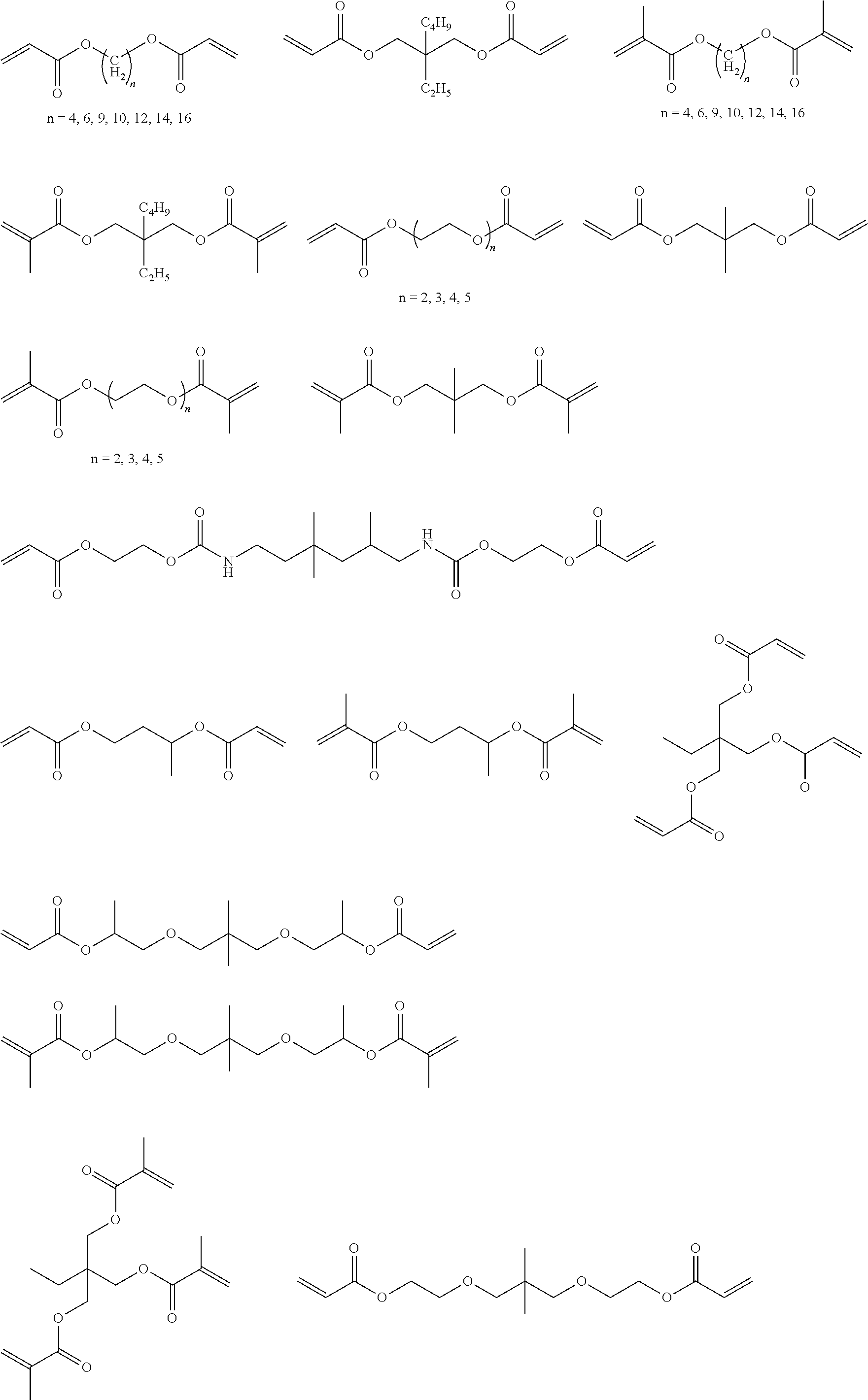
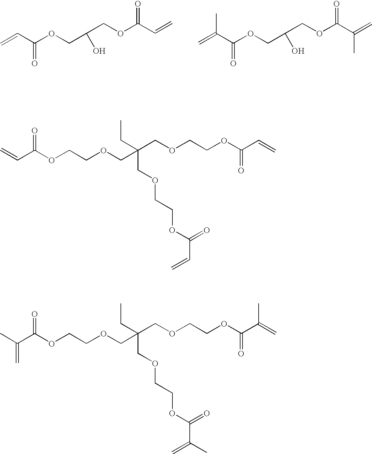
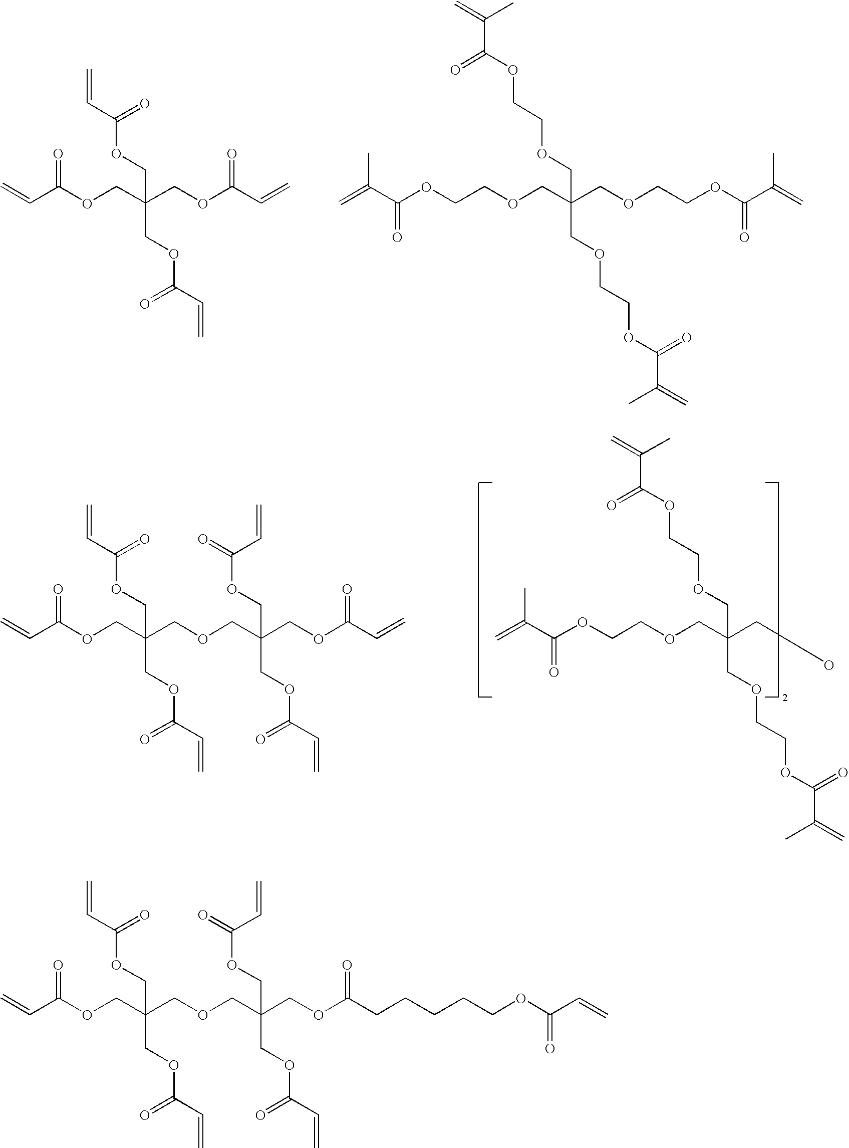
[0108]Gas barrier films (Samples Nos. 1 to 11) having an inorganic layer and an organic layer provided on a flexible supporting substrate were prepared according to the following procedures. Details of a structure of each of the gas barrier films are described in Table 1. A PEN (Q-65A, manufactured by Teijin DuPont Films Japan Limited) film having a thickness of 100 μm was used as the flexible supporting substrate.

(1) Formation of Inorganic Layer (X)

[0109]An inorganic layer was formed by a plasma CVD apparatus. A specific fabrication condition is shown below.

[0110]A vacuum chamber of the plasma CVD apparatus was evacuated to an ultimate pressure of 4×10⁻³ Pa by an oil-sealed rotary pump and a turbo-molecular pump. Next, argon was introduced as a discharge gas, and a discharge electric power of 500 W was applied from a discharge power source. A silane gas (SiH4) and nitrogen were introduced into the chamber, and the fabrication was carrie...

example 2

Preparation and Evaluation of Organic El Device

(1) Preparation of Organic EL Device

[0128]A conductive glass substrate having an ITO film (surface resistivity value: 10Ω / □) was rinsed with 2-propanol and then subjected to a UV-ozone treatment for 10 minutes. The following organic compound layers were successively vapor deposited on this substrate (anode) by a vacuum vapor deposition method.

(First Hole Transport Layer)

Copper phthalocyanine: thickness, 10 nm

(Second Hole Transport Layer)

N,N′-Diphenyl-N,N′-dinaphthylbenzidine: thickness, 40 nm

(Light-Emitting Layer / Electron Transport Layer)

Tris(8-hydroxyquinolinato)aluminum: thickness, 60 nm

[0129]Finally, 1 nm of lithium fluoride and 100 nm of metallic aluminum were successively vapor deposited to form a cathode, onto which was then applied a silicon nitride film having a thickness of 5 μm by a plane-parallel plate CVD method, thereby preparing an organic EL device.

(2) Installment of Gas Barrier Layer on Organic EL Device

[0130]Each of the...


PUM

PropertyMeasurementUnit
thicknessaaaaaaaaaa
heat resistanceaaaaaaaaaa
Tgaaaaaaaaaa

Abstract

A gas barrier film having a gas barrier layer and an antistatic layer containing an acrylic or methacrylic resin obtained by copolymerizing a monomer represented by the formula (1) or an oligomer thereof:(Ac1-L1)m-M-(L2-Ac2)  Formula (1)wherein Ac1 and Ac2 represent a (meth)acryloyl group; L1 and L2 represent an alkylene group, an arylene group, etc.; M represents a metal atom; m and n are an integer of 0-6; and the total sum of m and n is 1-6. The gas barrier film has high barrier properties.

Description

BACKGROUND OF THE INVENTION[0001]1. Field of the Invention[0002]The present invention relates to a film with excellent gas barrier properties and an organic device using the same, particularly a laminated gas barrier film which is suitable for substrates or covering films of various organic devices. Furthermore, the invention relates to an organic device with excellent durability and flexibility using the foregoing gas barrier film, particularly an organic EL device.[0003]2. Description of the Related Art[0004]In recent years, in organic devices such as liquid crystal display devices, solar cells and electroluminescent (EL) devices, the use of a transparent plastic film which is thin, light and excellent in flexibility in place of a glass substrate which is heavy and easy to break is being studied. In view of the matters that transparent plastic substrates are easy to realize a large area and able to be applied for a roll-to-roll production system, they are good in productivity as c...

Claims


Application Information

Patent Timeline
Patent Type & Authority Patents(United States)
IPC IPC(8): H01J1/63
CPCC09D4/00H01L51/5237H05B33/04Y10T428/1068Y10T428/1045Y10T428/1064Y10T428/31855C09K2323/033C09K2323/051C09K2323/053H10K50/8445
Inventor AIBA, SATOSHI
Owner FUJIFILM CORP
Why Eureka
Try Eureka