Glass flux assisted sintering of chemical solution deposited thin dielectric films

a technology of dielectric films and glass flux, which is applied in the direction of fixed capacitor details, fixed capacitors, liquid/solution decomposition chemical coatings, etc., can solve the problems of reducing the dielectric constant, achieving high densification levels,

Active Publication Date: 2012-05-22
CHEMTRON RES
View PDF4 Cites 5 Cited by
  • Summary
  • Abstract
  • Description
  • Claims
  • Application Information

AI Technical Summary

Problems solved by technology

Firing a CSD dielectric deposit on copper foil restricts the shrinkage to the “z” or vertical dimension when sintering takes place and combined with the high level of refractoriness exhibited by high dielectric constant materials, achieving high levels of densification is extremely difficult.
In addition to the reliability concerns, since air has a dielectric constant of 1, such levels of porosity will result in a reduction of the dielectric constant.
Thus, a problem to be solved in present electronic circuitry is the production of a dense CSD dielectric of a fired-on-foil capacitor while maintaining other desirable properties, such as high capacitance density.

Method used


Image

  • Glass flux assisted sintering of chemical solution deposited thin dielectric films
  • Glass flux assisted sintering of chemical solution deposited thin dielectric films
  • Glass flux assisted sintering of chemical solution deposited thin dielectric films

Examples


examples

[0071]The following examples illustrate useful properties in dielectric compositions and capacitors incorporating these compositions, prepared according to the methods described herein. In the examples below, when an amount, concentration, or other value or parameter is given as a range, as one or more preferred ranges or as a list of upper preferable values and lower preferable values, this is to be understood as specifically disclosing all ranges formed from any pair of any upper range limit or preferred value and any lower range limit or preferred value, regardless of whether such pairs are separately disclosed.

examples 1-3

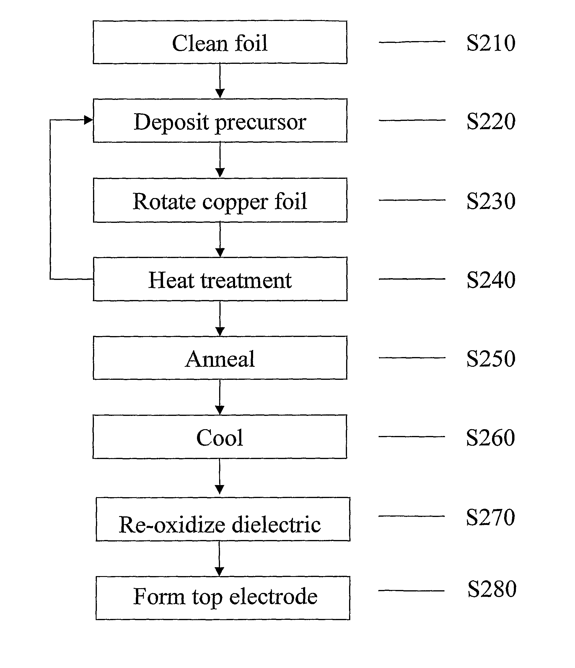
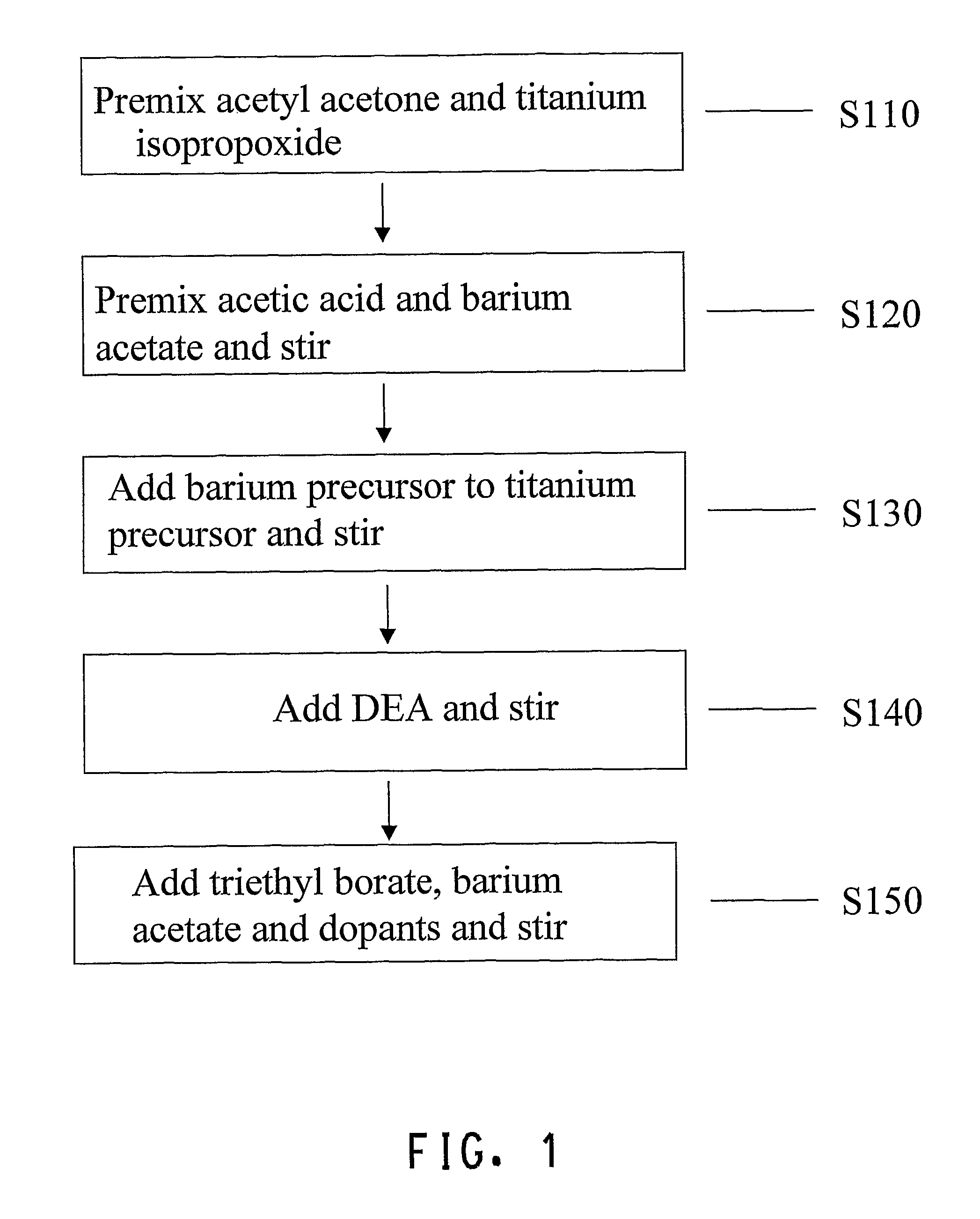
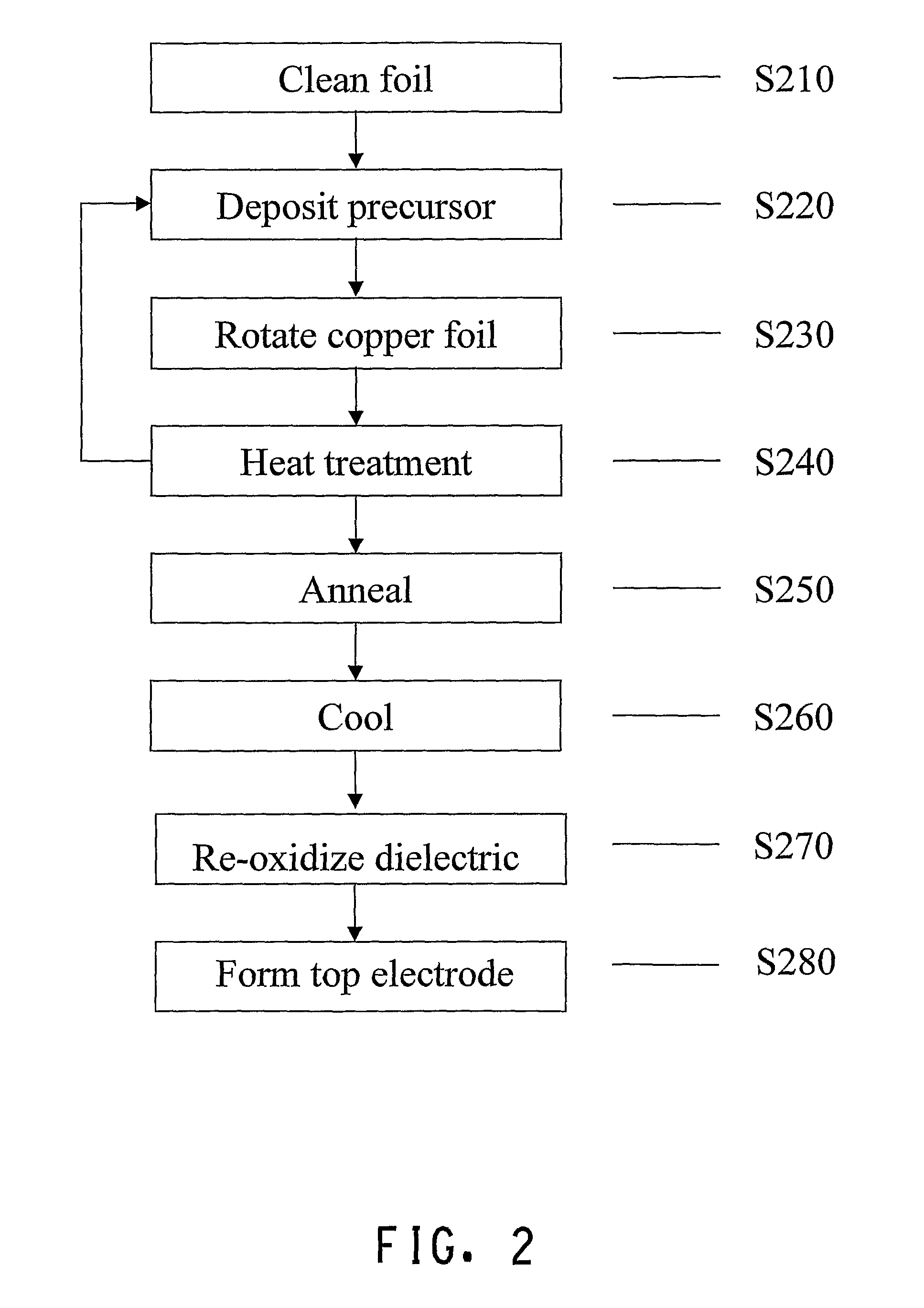
[0072]Barium titanate thin-film capacitors were prepared on copper foil using the process as depicted in FIG. 2. The precursor compositions contained 0, 0.69, and 1.38 mole % boron oxide glass flux additions by addition of the appropriate amounts of triethyl borate to the barium titanate solution. Annealing was performed at 900° C. for 30 minutes, under an atmosphere of a partial pressure of oxygen of 10−12 atmospheres. The dielectric compositions were re-oxygenated after the annealing process for 30 minutes at 450° C., under a partial pressure of oxygen of 10−4 atmospheres. The resultant maximum dielectric constants or relative permittivities of the barium titanate films were approximately 1600, 2250, and a little less than 3000 for 0, 0.69, and 1.38 mole % boron oxide respectively as shown in FIG. 4. The relative permittivity and loss factor versus field strength of the barium titanate film containing an addition of 1.38 mole % boron oxide flux is shown in FIG. 5. Cross sectional ...

examples 4-6

[0073]Barium titanate thin-film capacitors were prepared on copper foil using the process as described in FIG. 2. The compositions contained 0, 1.5, and 3.0 mole % boron oxide glass flux additions by addition of the appropriate amounts of tri-n-butylborate to the barium titanate solution Annealing was performed at 900° C. for 30 minutes, under an atmosphere of a partial pressure of oxygen of 10−12 atmospheres. Cross-sections of the dielectrics were made and focused ion beam (FIB) images were taken of the cross-sections to show the porosity level. The images are shown in FIG. 7 (a-c) wherein the dielectric layer is identified by the marker 700.


PUM

PropertyMeasurementUnit
dielectric constantaaaaaaaaaa
thicknessaaaaaaaaaa
thicknessaaaaaaaaaa

Abstract

A method of making dense dielectrics layers via chemical solution deposition by adding inorganic glass fluxed material to high dielectric constant compositions, depositing the resultant mixture onto a substrate and annealing the substrate at temperatures between the softening point of the inorganic glass flux and the melting point of the substrate. A method of making a capacitor comprising a dense dielectric layer.

Description

BACKGROUND[0001]1. Technical Field[0002]The technical field is embedded capacitors, particularly capacitors having thin film dielectrics.[0003]2. Related Art[0004]The practice of embedding capacitors in printed wiring boards (PWB) allows for reduced circuit size and improved circuit performance. Capacitors are typically embedded in panels that are stacked and connected by interconnection circuitry, the stack of panels forming a printed wiring board.[0005]Fired-on-foil thin-film capacitor technology is known. U.S. Pat. No. 7,029,971 to Borland et al. discloses a chemical solution deposition (CSD) fired-on-foil thin-film process in which fired-on-foil thin-film CSD capacitors are formed by first depositing a thin capacitor dielectric precursor material layer onto a metallic foil substrate, typically by spin coating. Several spin-coated layers may be utilized. The metallic foil substrate may be copper foil and typically may range in thickness between 12 and 36 microns. The deposited CS...

Claims


Application Information

Patent Timeline
Patent Type & Authority Patents(United States)
IPC IPC(8): H01L21/20H01B3/20H01B3/00
CPCC23C18/1212C23C18/1241C23C18/1266C23C18/1283C23C18/1295H01G4/129H01L21/31691H05K1/162H05K2201/017H05K2201/0355H01L21/02197H01L21/02282H01L21/02356H01L21/02337
Inventor BORLAND, WILLIAM J.SUH, SEIGIMARIA, JON-PAULIHLEFELD, JON FREDRICKBURN, IAN
Owner CHEMTRON RES
Why Eureka
Try Eureka