Thin film transistor, manufacturing method thereof, and semiconductor device

a thin film transistor and manufacturing method technology, applied in the field of thin film transistors, can solve the problems of dramatic improvement in the electron field-effect mobility of semiconductor films, and the attention of continuous oscillation lasers, so as to achieve the effects of improving the mobility of carriers in the semiconductor layer of a tft, reducing the boundary of crystal grains, and improving the mobility of polycrystalline semiconductor layers

Active Publication Date: 2012-07-03
SEMICON ENERGY LAB CO LTD
View PDF19 Cites 7 Cited by
  • Summary
  • Abstract
  • Description
  • Claims
  • Application Information

AI Technical Summary

Benefits of technology

[0011]Lasers are largely classified into two types, pulsed oscillation or continuous oscillation, according to their oscillation methods. Since a pulsed laser has relatively high output energy, productivity can be improved with a size of laser light (a region in a surface of an object to be treated that is actually irradiated with laser light) of several cm2 or larger. In particular, by processing a shape of the irradiation region of the laser light by an optical system to make it linear with a length of 10 cm or longer, laser light irradiation of the substrate can be performed efficiently, and productivity can be improved even more. Consequently, pulsed lasers have been becoming the mainstream in crystallization of semiconductor films.
[0014]An object of the present invention is to provide a semiconductor device with high carrier mobility and a favorable electrical characteristic, and a manufacturing method thereof.
[0047]By the present invention, a direction of crystal growth can be controlled. Therefore, crystal grain boundaries can be reduced. Accordingly, mobility of a polycrystalline semiconductor layer can be spectacularly improved.
[0048]By the present invention, because mobility of carriers in a semiconductor layer of a TFT is improved, a TFT having a favorable electrical characteristic can be manufactured.
[0049]Since a TFT having a favorable electrical characteristic can be manufactured by the present invention, a circuit element with higher performance than before can be formed. Accordingly, a semiconductor device with more added value than before can be manufactured over a glass substrate.

Problems solved by technology

Consequently, the continuous oscillation laser is receiving a lot of attention.
Therefore, it does not lead to a dramatic improvement in electron field-effect mobility of semiconductor films.

Method used


Image

  • Thin film transistor, manufacturing method thereof, and semiconductor device
  • Thin film transistor, manufacturing method thereof, and semiconductor device
  • Thin film transistor, manufacturing method thereof, and semiconductor device

Examples


embodiment mode 1

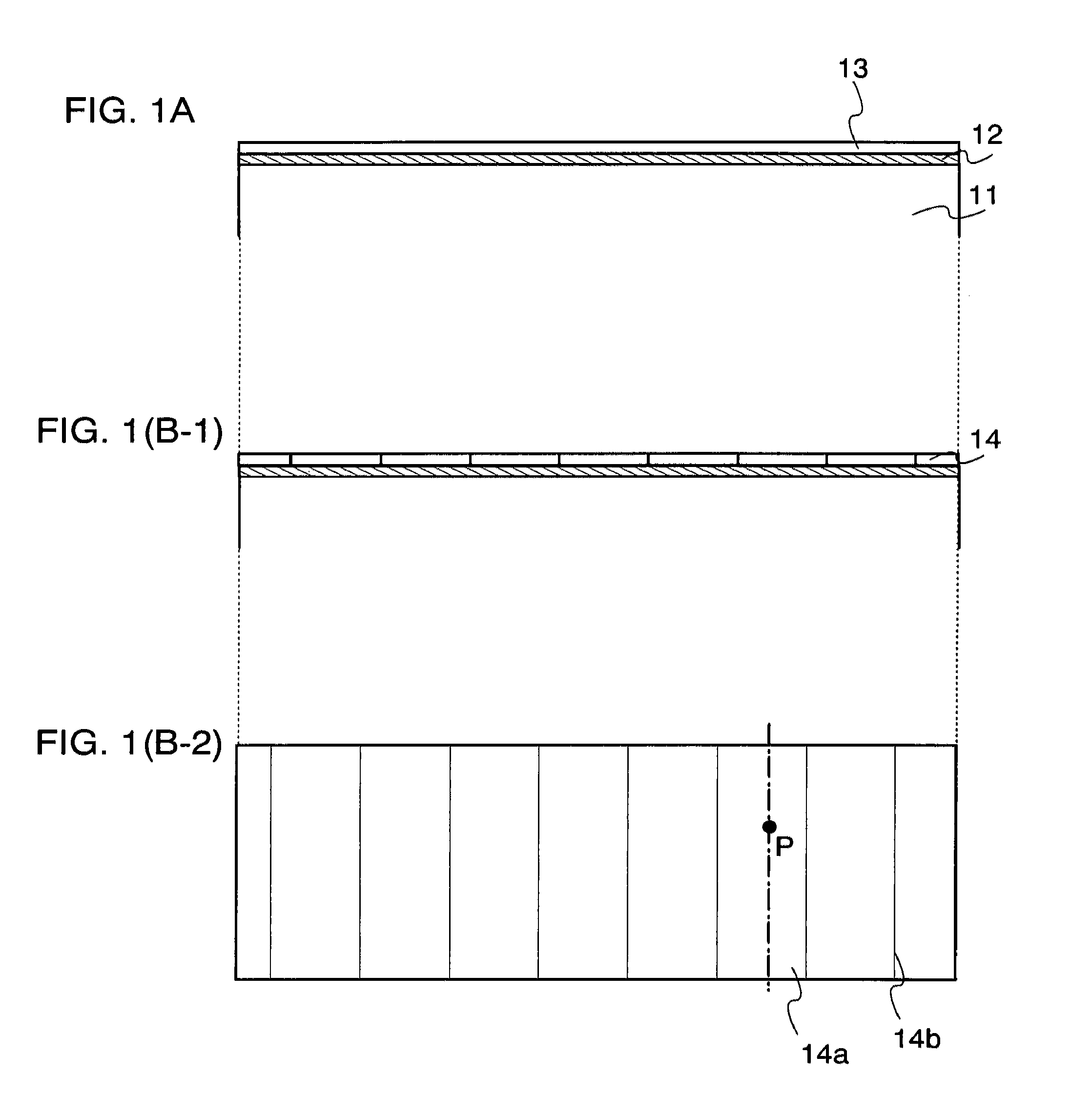
[0085]In this embodiment mode, a forming process of a semiconductor layer included in a semiconductor device to which the present invention is applied is described with reference to FIGS. 1 to 6. FIG. 1 shows a process up to forming a polycrystalline semiconductor film over a substrate, which is described in this embodiment mode.

[0086]For a substrate, a glass substrate 11 is used as an insulating substrate. A material of the glass substrate 11 is not particularly limited, and quartz glass, alkali-free glass such as borosilicate glass, or alumino silicate glass may be used, provided that it has heat resistance, chemical resistance, and the like necessary in a step of forming a thin film thereafter. Note that not only a glass substrate is used, and a material of the substrate is not particularly limited provided that a substrate surface has an insulating property and has the necessary heat resistance. That is, a plastic substrate having enough heat resistance that can withstand a temp...

embodiment mode 2

[0150]In this embodiment mode, an example of a manufacturing process of a TFT in a liquid crystal display device to which the present invention is applied is described with reference to FIGS. 7A to 10B. FIGS. 7A to 10B show TFTs (pixel TFTs) included in a pixel portion of a liquid crystal display device. In FIGS. 7A, 8A, 9A, and 10A, top views are shown, and FIGS. 7B, 8B, 9B, and 10B show cross-sectional diagrams along a line connecting X1 to X3 in FIGS. 7A, 8A, 9A, and 10A, respectively.

[0151]In this embodiment mode, a glass substrate 70 is used as a substrate. A base layer 71 is formed over the glass substrate 70. An amorphous silicon film is formed over the base layer 71. The base layer 71 may be formed of a silicon oxide based material or a silicon nitride based material. Alternatively, the base layer 71 may have a structure in which films made of such materials are stacked. Favorably, the base layer 71 may have a stacked layer structure of two layers in which a silicon oxide fi...

embodiment mode 3

[0183]In this embodiment mode, a light-emitting element in Embodiment Mode 2 is described.

[0184]Next, an EL display device manufactured by applying the present invention is described with reference to FIGS. 12A to 12C. When an N-type transistor is used as a transistor that drives a light-emitting element, light emitted from the light-emitting element is emitted by any manner of bottom emission (see FIG. 12A), top emission (see FIG. 12B), or dual emission (FIG. 12C). By using a TFT 451, a TFT 461, and a TFT 471, an electric field to light-emitting layers connected to the TFTs are controlled. A light-emitting layer 452, a light-emitting layer 462, and a light-emitting layer 472 are electric field light-emitting layers, and an EL may be sued. Light-emitting elements using EL are categorized by whether a light-emitting material is an organic compound or an inorganic compound, and in general, the former is called an organic EL element and the latter is called an inorganic EL element. Her...


PUM

PropertyMeasurementUnit
temperatureaaaaaaaaaa
lengthaaaaaaaaaa

Abstract

By a laser crystallization method, a crystalline semiconductor film in which grain boundaries are all in one direction is provided as well as a manufacturing method thereof. In crystallizing a semiconductor film formed over a substrate with linear laser light, a phase-shift mask in which trenches are formed in a stripe form is used. The stripe-form trenches formed in the phase-shift mask are formed so as to make a nearly perpendicular angle with a major axis direction of the linear laser light. CW laser light is used as the laser light, and a scanning direction of the laser light is nearly parallel to a direction of the stripe-form trenches (grooves). By changing luminance of the laser light periodically in the major axis direction, a crystal nucleation position in a semiconductor that is completely melted can be controlled.

Description

BACKGROUND OF THE INVENTION[0001]1. Field of the Invention[0002]The present invention relates to a semiconductor device and a manufacturing method thereof. In particular, the present invention relates to a semiconductor device including a crystalline thin film transistor and a manufacturing method thereof. Further, the present invention relates to a semiconductor device and an electronic appliance mounted with the thin film transistor.[0003]2. Description of the Related Art[0004]In recent years, development of techniques regarding semiconductor devices including thin film transistors (hereinafter referred to as “TFT”) has been actively pursued. In particular, application to active matrix type display devices and the like using a glass substrate has been advanced.[0005]Semiconductor films used for TFTs can be largely classified into those with crystalline (polycrystalline) structures and those with amorphous structures. TFTs using semiconductor films of the polycrystalline structure ...

Claims


Application Information

Patent Timeline
Patent Type & Authority Patents(United States)
IPC IPC(8): H01L29/10H01L29/76H01L31/036H01L31/112
CPCB23K26/0626H01L29/78696B23K26/0738B23K26/0884H01L21/02532H01L21/02678H01L21/02683H01L21/02691H01L29/04H01L29/66757H01L29/78675B23K26/0656B23K2201/006H01L27/1285H01L27/1296B23K26/066B23K2101/006
Inventor MIYAIRI, HIDEKAZU
Owner SEMICON ENERGY LAB CO LTD
Why Eureka
Try Eureka