Nanowire sensor, nanowire sensor array and method of fabricating the same

a nanowire sensor and nanowire technology, applied in the field of sensors, can solve the problems of limited research based on “bottom-up” nanostructure, difficulty in delivering biological receptors such as enzymes, antibodies, proteins or biologicals, and achieve the effect of reducing production costs and easy and cost-effective methods of producing sensors

Inactive Publication Date: 2012-08-07
AGENCY FOR SCI TECH & RES
View PDF21 Cites 9 Cited by
  • Summary
  • Abstract
  • Description
  • Claims
  • Application Information

AI Technical Summary

Benefits of technology

[0008]The invention provides a method of fabricating a sensor comprising a nanowire on a support substrate with a first semiconductor layer arranged on the support substrate. The method comprises forming a fin structure from the first semiconductor layer, the fin structure comprising at least two supporting portions and a fin portion arranged there between; oxidizing at least the fin portion of the fin structure thereby forming the nanowire being surrounded by a first layer of oxide; and forming a first insulating layer above the supporting portions; wherein the supporting portions and the first insulating layer form a microfluidic channel. This method can provide an easy and cost effective manner to produce sensors since the method is fully compatible with conventional Si (CMOS) technology and can be carried out in a standard Si foundry. This also means that other CMOS circuitry can be built alongside for signal processing, thereby allowing scalability and reducing production costs.
[0011]In one embodiment of the invention, the method further comprises forming a second layer of oxide on a contact surface of the supporting portions before forming the first insulating layer. The second layer of oxide is typically silicon oxide but not so limited. The second layer of oxide can be about 0.2 micron to about 1 micron thick and is thicker than the first layer of oxide surrounding the nanowire. The second layer of oxide serves to protect the supporting portions for subsequent deposition.

Problems solved by technology

However, most of the existing studies based on “bottom-up” nanostructures are limited by complex integration, requiring transfer and positioning of an individual nanostructure, making reliable ohmic contacts and the control of doping concentrations.
In addition, delivery of a biological receptor such as enzymes, antibodies, proteins or biological macromolecules that can be used for detection of an analyte remains a challenge in nanostructure sensor devices.
Currently, delivery is normally accomplished by using syringe pumps, micropipettes or atomic force microscopy (AFM) tips (Dip-pen) which is crude, time-consuming and trial and error based, as there is a need to accurately locate the nanowire with precision.
Therefore, such delivery methods are only meant for laboratory experiments and are not useful from a product realization point of view.
Fabricating the prior art devices as mentioned above is rather cumbersome and expensive.

Method used


Image

  • Nanowire sensor, nanowire sensor array and method of fabricating the same
  • Nanowire sensor, nanowire sensor array and method of fabricating the same
  • Nanowire sensor, nanowire sensor array and method of fabricating the same

Examples


experimental examples

[0124]A method of fabricating a sensor comprising a nanowire on a support substrate with a semiconductor layer arranged on the support substrate according to one embodiment of the present invention is set forth hereunder based on the following experimental examples. However, they should not be construed as limiting the scope of this invention.

example 1

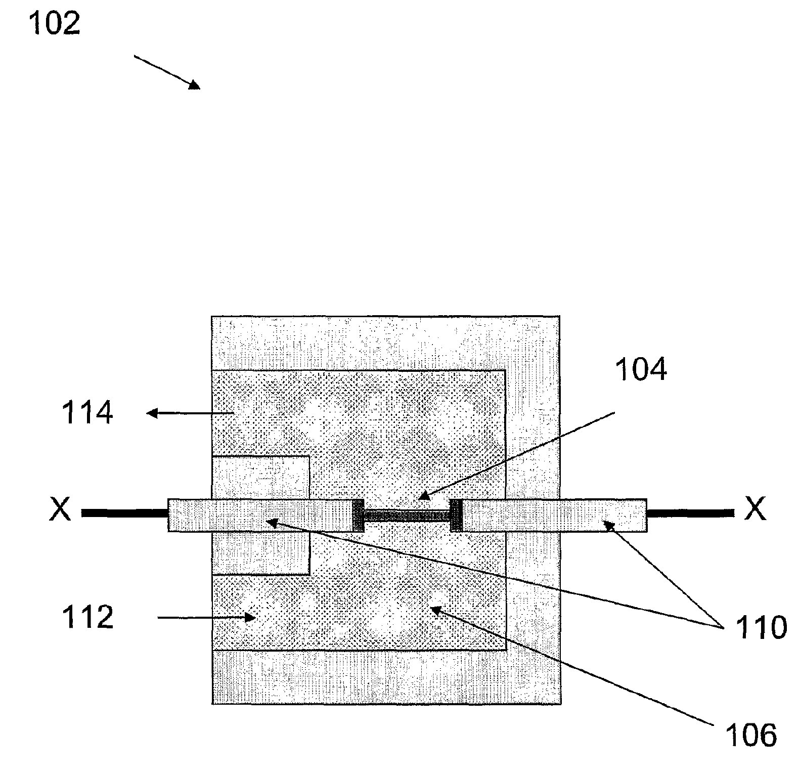
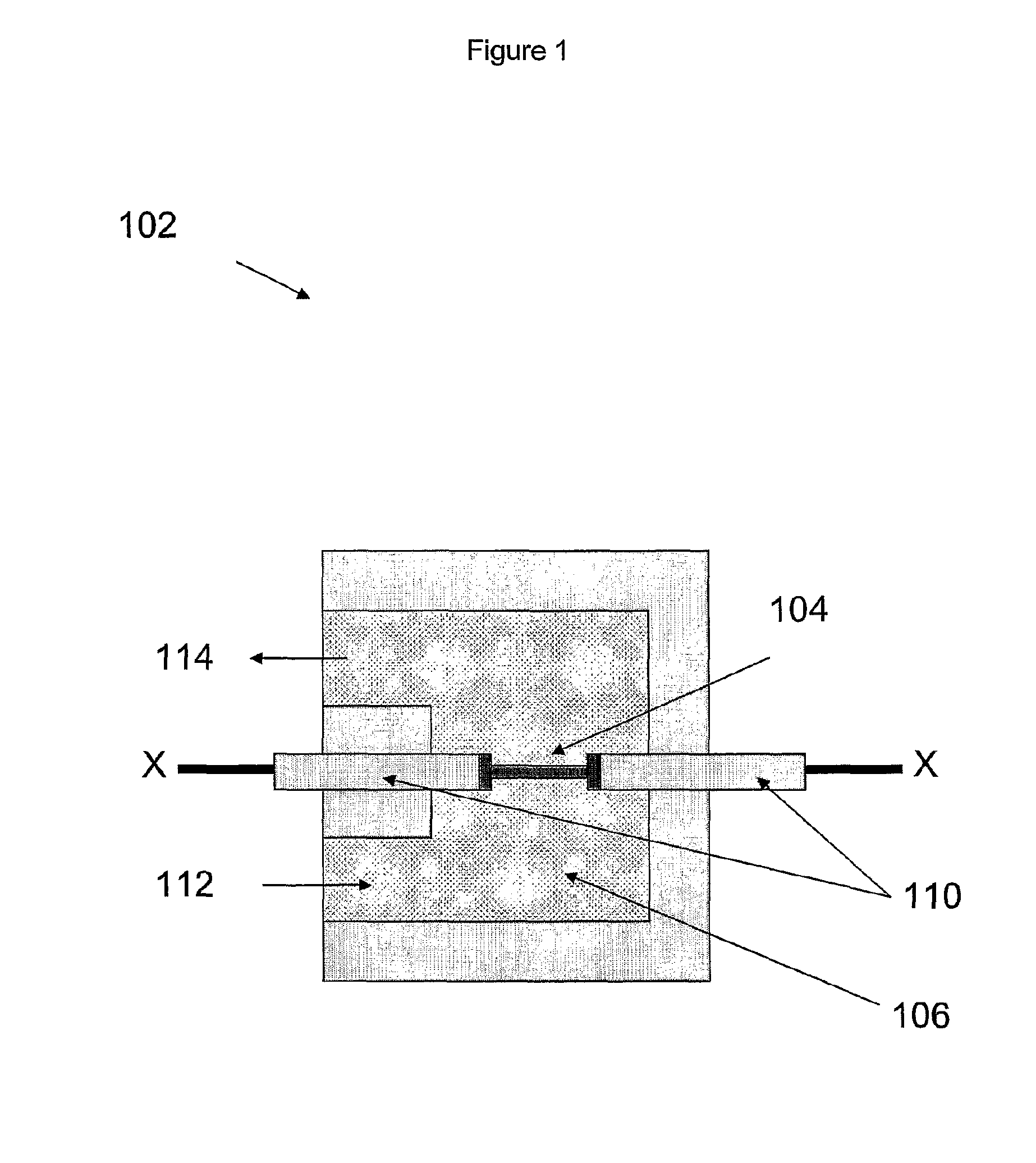
[0125]For Si nanowire formation, SOI wafers of 200 mm diameter consisting of 200 nm thick Si device layer and 150 nm thick BOX on support substrate were utilized. Trenches were formed in Si device layer up to the BOX by lithography and etching to obtain Si FINs of width 80 nm. The wafers were then oxidized in dry O2 ambient at 900° C. for 6 hrs to form nanowires 104 as shown in FIG. 15. The single nanowire is one of the nanowire structural arrangements mentioned in FIG. 6A. By doping n-type, p-type or a combination of n-type and p-type dopants, nanowires of different functional types can be realized as mentioned in FIG. 7A and FIG. 7B.

example 2

[0126]The High Resolution Transmission Electron Microscopy (HRTEM) images of Si nanowires are shown in FIG. 16A and FIG. 16B. FIG. 16A shows a nanowire 172 with a triangular cross-section with base 200 of about 10 nanometers and height 202 of about 12.3 nanometers. The reason for the triangular shape results from different oxidation fronts along various crystallographic orientations. By using the visco-elastic properties of SiO2 and Si atomic migration at the Si—SiO2 interface, a circular shape transformation can also be brought about by subjecting the wafers to nitrogen (N2) anneal at approximately 1200° C. for 1 hr. A nanowire 174 with a circular cross-section with a diameter of about 7.7 nanometers is shown in FIG. 16B. Therefore, the cross-section of the nanowire can be triangular or circular depending on the process conditions.

[0127]A nanowire sensor array comprising a plurality of nanowire sensors wherein each nanowire sensor is individually addressable via the supporting port...


PUM

PropertyMeasurementUnit
thickaaaaaaaaaa
thicknessaaaaaaaaaa
thicknessaaaaaaaaaa

Abstract

A method of fabricating a sensor comprising a nanowire on a support substrate with a first semiconductor layer arranged on the support substrate is disclosed. The method comprises forming a fin structure from the first semiconductor layer, the fin structure comprising at least two supporting portions and a fin portion arranged there between; oxidizing at least the fin portion of the fin structure thereby forming the nanowire being surrounded by a first layer of oxide; and forming an insulating layer above the supporting portions; wherein the supporting portions and the first insulating layer form a microfluidic channel. A nanowire sensor is also disclosed. The nanowire sensor comprises a support substrate, a semiconducting fin structure arranged on the support substrate, the fin structure comprising at least two semiconducting supporting portions and a nanowire arranged there between; and a first insulating layer on a contact surface of the supporting portions; wherein the supporting portions and the first insulating layer form a microfluidic channel.

Description

FIELD OF THE INVENTION[0001]The present invention relates to the field of sensors, and in particular, to a method of fabricating a sensor comprising a nanowire on a support substrate with a semiconductor layer arranged on the support substrate. The present invention also relates to a nanowire sensor and a nanowire sensor array.BACKGROUND OF THE INVENTION[0002]One-dimensional nanostructures such as nanowires and carbon nanotubes are known to be promising candidates for highly sensitive and miniaturized molecular sensors. In particular, sensors based upon semiconductor nanostructures, such as carbon nanotubes, silicon (Si) nanowires, tin oxide (SnO2) nanowires, and indium oxide (In2O3) nanowires, are particularly promising as their detection is based on the principle of a change in surface charge of the nanostructures in the presence or absence of molecular species.[0003]Due to a high surface-to-volume ratio of nanowires, their electronic conductance may be sensitive enough to the sur...

Claims


Application Information

Patent Timeline
Patent Type & Authority Patents(United States)
IPC IPC(8): H01L21/00
CPCB01J19/0046B81C1/00119B82Y15/00C40B60/12B01J2219/00497B01J2219/00527B01J2219/00585B01J2219/00596B01J2219/00612B01J2219/00653B01J2219/00659B01J2219/00677B01J2219/00722B01J2219/00725B01J2219/00729B81B2201/0214B81B2203/0338B81B2207/07Y10S977/957Y10S977/958
Inventor AGARWAL, AJAYSINGH, NAVABKUMAR, RAKESHLAO, IENG KINBALASUBRAMANIAN, NARAYANAN
Owner AGENCY FOR SCI TECH & RES
Why Eureka
Try Eureka