Method of processing synthetic quartz glass substrate for semiconductor

a technology of synthetic quartz glass and substrate, which is applied in the direction of grinding heads, manufacturing tools, lapping machines, etc., can solve the problems of inability to form recipes for flatness improvement, and inability to form fine patterns, etc., to achieve excellent flatness and improve flatness

Active Publication Date: 2013-01-29
SHIN ETSU CHEM IND CO LTD
View PDF30 Cites 6 Cited by
  • Summary
  • Abstract
  • Description
  • Claims
  • Application Information

AI Technical Summary

Benefits of technology

[0030]When the processing method according to the present invention is applied to the production of a synthetic quartz glass such as one for a photomask substrate for use in photolithography which is important to the manufacture of ICs or the like, a substrate which has an extremely excellent flatness and is capable of coping even with the EUV lithography can be obtained comparatively easily and inexpensively.
[0031]In addition, when the small-sized processing tool having the above-mentioned specified hardness is used, it is possible to obtain a substrate having an improved flatness which has few defects such as polish flaw.

Problems solved by technology

In fact, if the exposure surface is not flat at the time of exposure, a shift of focus on the silicon wafer would be generated to worsen the pattern uniformity, making it impossible to form a fine pattern.
Even if a substrate with a flatness of less than 0.3 μm could be obtained, the yield of such a substrate would necessarily be extremely low.
The reason lies in that according to the conventional polishing technology, it is practically impossible to form recipes of flatness improvement based on the shapes of raw material substrates and to individually polish the substrates for improving the flatness, although it is possible to generally control the polishing rate over the whole surface of each substrate.
Besides, for example, in the case of using a double side polishing machine of a batch processing type, it is extremely difficult to control the within-batch and batch-to-batch variations of flatness.
In either case, therefore, it has been difficult to stably produce excellently flat substrates.
In the cases of improving the flatness of a substrate surface by use of these novel technologies, however, there are such problems as large or intricate equipment and raised processing costs.
For example, in the cases of plasma etching and gas cluster ion etching, the processing apparatus would be expensive and large in size, and many auxiliary equipments such as an etching gas supplying equipment, a vacuum chamber and a vacuum pump are needed.
Furthermore, when depreciation expenses of the equipments and the costs of expendables, such as expensive gases (e.g., SF6) consumed in each run of processing, are passed onto the price of the mask-forming glass substrate, the improved-flatness substrate would necessarily be high in price.
In the lithography industry, also, the substantial rise in the price of masks is deemed as a significant problem.
Therefore, a rise in the price of the glass substrates for masks is undesirable.
In this method, however, the pressing is from the back side of the substrate, so that the polishing action would not reach a protuberant portion of the face-side surface locally and effectively.
Accordingly, the use of this flatness-improving method alone is insufficient in capability as a technology for producing a mask of the EUV lithography generation.

Method used


Image

  • Method of processing synthetic quartz glass substrate for semiconductor
  • Method of processing synthetic quartz glass substrate for semiconductor
  • Method of processing synthetic quartz glass substrate for semiconductor

Examples


example 1

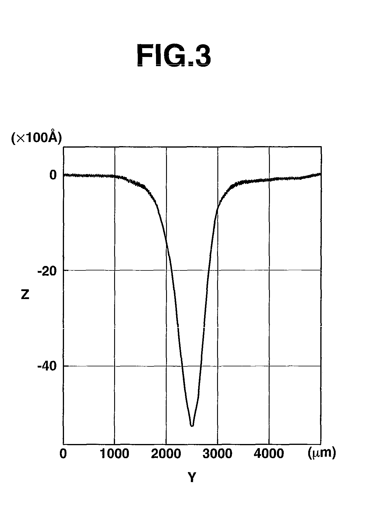
[0070]A sliced silica synthetic quartz glass substrate raw material (6 in) was subjected to lapping by use of a double side lapping machine designed for sun-and-planet motion, and was subjected to rough polishing by use of a double side polishing machine designed for sun-and-planet motion, to prepare a raw material substrate. In this instance, the surface flatness of the raw material substrate was 0.314 μm. Incidentally, measurement of flatness was conducted by use of a flatness measuring system Ultra Flat M200, produced by Tropel Corp. Then, the glass substrate was mounted on a substrate holder of an apparatus shown in FIG. 9. In this case, the apparatus had a structure in which a processing tool 2 is attached to a motor and can be rotated, and a pressure can be pneumatically applied to the processing tool 2. In FIG. 9, numeral 7 denotes a pressing precision cylinder, and numeral 8 denotes a pressure controlling regulator. As the motor, a small-sized grinder (produced by Nihon Seim...

example 2

[0078]A sliced silica synthetic quartz glass substrate raw material (6 in) was subjected to lapping by use of a double side lapping machine designed for sun-and-planet motion, and was subjected to rough polishing by use of a double side polishing machine designed for sun-and-planet motion, to prepare a raw material substrate. In this instance, the surface flatness of the raw material substrate was 0.328 μm. Then, the glass substrate was mounted on the substrate holder of the apparatus shown in FIG. 9. As the processing tool, one in which a polishing part having an exclusive-use felt disc (A4021, produced by Nihon Seimitsu Kikai Kosaku Co., Ltd.; hardness: A65) adhered to a 20 mmφ soft rubber pad (A3020, produced by Nihon Seimitsu Kikai Kosaku Co., Ltd.) was used. The tool has a mechanism in which it is perpendicularly pressed against the substrate surface, the contact area being 314 mm2.

[0079]Next, the processing tool was moved on the work under a rotational speed of 4,000 rpm and a...

example 3

[0081]A sliced silica synthetic quartz glass substrate raw material (6 in) was subjected to lapping by use of a double side lapping machine designed for sun-and-planet motion, and was subjected to rough polishing by use of a double side polishing machine designed for sun-and-planet motion, to prepare a raw material substrate. In this instance, the surface flatness of the raw material substrate was 0.350 μm. Then, the glass substrate was mounted on the substrate holder of the apparatus shown in FIG. 9. As the processing tool, one in which a polishing part having an exclusive-use felt disc (A4011, produced by Nihon Seimitsu Kikai Kosaku Co., Ltd.; hardness: A65) adhered to a 10 mmφ soft rubber pad (A3010, produced by Nihon Seimitsu Kikai Kosaku Co., Ltd.) was used. The tool has a mechanism in which it is perpendicularly pressed against the substrate surface, the contact area being 78.5 mm2.

[0082]Next, the processing tool was moved on the work under a rotational speed of 4,000 rpm and ...


PUM

PropertyMeasurementUnit
areaaaaaaaaaaa
angleaaaaaaaaaa
flatness F2aaaaaaaaaa

Abstract

Disclosed is a method of processing a synthetic quartz glass substrate for a semiconductor, wherein a polishing part of a rotary small-sized processing tool is put in contact with a surface of the synthetic quartz glass substrate in a contact area of 1 to 500 mm2, and is scanningly moved on the substrate surface while being rotated so as to polish the substrate surface. When the method is applied to the production of a synthetic quartz glass such as one for a photomask substrate for use in photolithography which is important to the manufacture of ICs or the like, a substrate having an extremely excellent flatness and capable of being used even with the EUV lithography can be obtained comparatively easily and inexpensively.

Description

CROSS-REFERENCE TO RELATED APPLICATION[0001]This non-provisional application claims priority under 35 U.S.C.§119(a) on Patent Application Nos. 2009-015542 and 2009-189393 filed in Japan on Jan. 27, 2009 and Aug. 18, 2009, respectively, the entire contents of which are hereby incorporated by reference.TECHNICAL FIELD[0002]The present invention relates to a method of processing a synthetic quartz glass substrate for a semiconductor, particularly a silica glass substrate for a reticle and a glass substrate for a nano-imprint, which are materials for most advanced applications, among semiconductor-related electronic materials.BACKGROUND ART[0003]Examples of quality of a synthetic quartz glass substrate include the size and density of defects on the substrate, flatness of the substrate, surface roughness of the substrate, photochemical stability of the substrate material, and chemical stability of the substrate surface. Requirements in regard of these qualities have been becoming severer...

Claims


Application Information

Patent Timeline
Patent Type & Authority Patents(United States)
IPC IPC(8): B24B1/00B24B7/24B24B37/07C03C19/00
CPCB24B7/241B24B41/053B24B13/0018
Inventor HARADA, DAIJITSUTAKEUCHI, MASAKIMATSUI, HARUNOBU
Owner SHIN ETSU CHEM IND CO LTD
Why Eureka
Try Eureka