
Manufacturing methods for metal clad laminates

a manufacturing method and metal clad technology, applied in the direction of superimposed coating process, transportation and packaging, coatings, etc., can solve the problems of reducing the adhesive power of continuous process, reducing the adhesive power of whole substrate, and bending and curled up whole substrates, etc., to achieve great hygroscopic

Active Publication Date: 2014-07-01
INKTEC CO LTD
View PDF27 Cites 11 Cited by
  • Summary
  • Abstract
  • Description
  • Claims
  • Application Information

AI Technical Summary

Benefits of technology

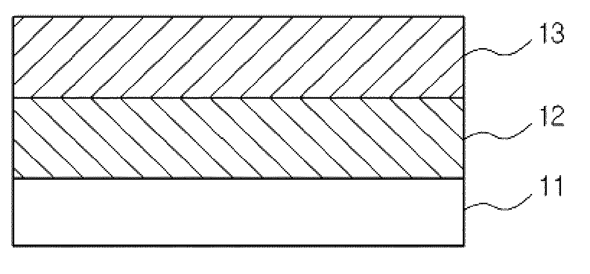
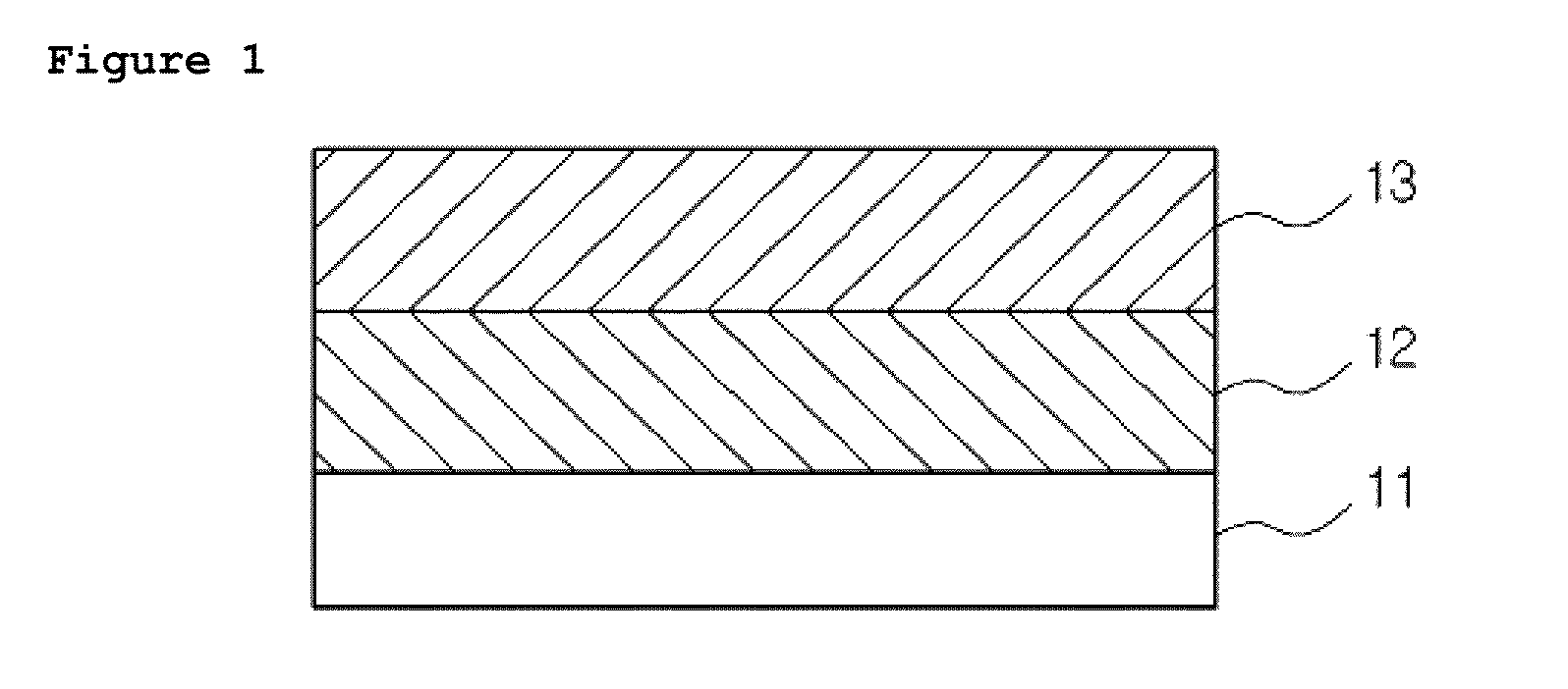
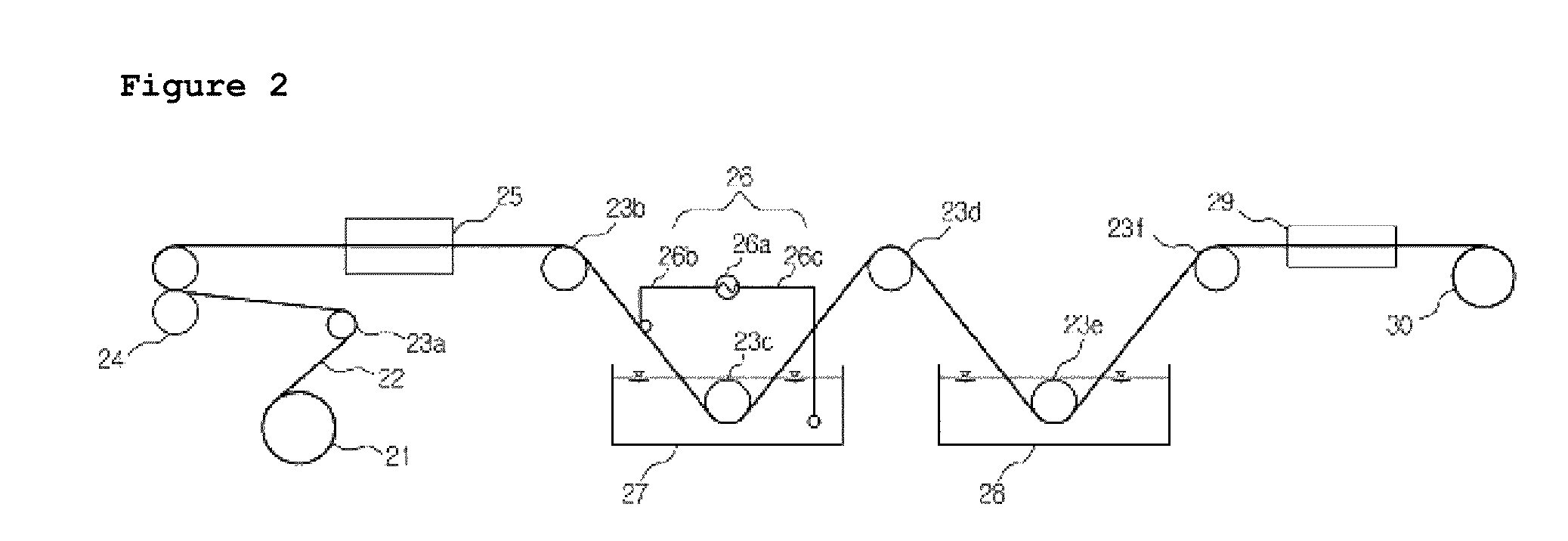
[0013]The present invention provides the manufacturing methods of metal clad laminates by forming a conductive layer on a single side or both sides of a material film that is made of an insulating material using the silver complexes having a unique structure and electroplating metals outside of said conductive layer. Also, the present invention provides the manufacturing methods of metal clad laminates, which form a conductive pattern layer by printing the silver coating composition comprising silver complexes having a unique structure directly on materials when forming said conductive layer and produce a low-resistance metal pattern layer.
[0014]Moreover, the present invention provides the manufacturing methods of metal clad laminates, which has a fast operation speed for mass production, simple process steps to minimize defective ratio and cheap production cost.Technical Solution
[0020]Also, for the present invention, the process inducing hydrophilicity can be used if necessary, through plasma treatment by inducing argon, oxygen, and nitrogen respectively or mixed gas of argon and oxygen; argon and nitrogen; or nitrogen and oxygen, so that it can improve adhesive power between the insulating materials and conductive layers.
[0038]Also, binder resins can be used to improve adhesive power between silver coating composition and the materials. The binder resins used here are acrylic resins such as polyacrylic acid or polyacrylic acid ester; cellulose based resins such as ethyl cellulose, cellulose ester, and cellulose nitrate; aliphatic or copolymer polyester based resins; vinyl based resins such as polyvinylbutyral, polyvinylacetate, polyvinylpyrrolidone; polyamide resins; polyurethane resins; polyether and urea resins; alkyd resins; silicone resins; fluoride resins; olefin based resins such as polyethylene or polystyrene; thermoplastic resins such as petroleum and rosin based resins; epoxy based resins; unsaturated or vinyl polyester based resins; diallylphthalate based resins; phenol based resins; oxetane based resins; oxazine based resins; bismaleimide based resins; modified silicone resins such as silicone epoxy or silicone polyester; thermosetting resins such as melamine based resin; acryl based resins with various structures of UV or electron-beam curing; natural polymer such as ethylene-propylene rubber (EPR), styrene-butadiene rubber (SBR), starch, and gelatin. One or more of these can be chosen and used together. Also, there can be not only organic resin binders but also inorganic binders such as glass resins or glass frit; silane coupling agents such as trimethoxy propyl silane or vinyl triethoxy silane; titanium, zirconium or aluminum based coupling agents.
[0055]As in FIG. 7, the cathode (71a, 71b) of the plating cartridge (70) plays a roll in contacting conductive patterns. For flexibility improvement, flexible plates (78) such as rubber and silicone are used as the material of inside of the cathode (71a, 71b). The inside of the plating cartridge (70) is filled with sponge (73), which has great hygroscopic. The sponge (73) is made to contact the anode (72) and cathode (71a, 71b) and its inside contains an electrode bar (79) that is used as anode (72). Inside of this electrode bar (79), there is an oscillator (75) that helps the plating solution flowing to the cathode (71a, 71b), which contacts the conductive pattern of the materials, by oscillating. Between the oscillator (75) and the electrode bar (79), there is an insulating layer to prohibit welding current. Also, in the upper part, the plating solution storage (77) is located to keep plating solution, which is transferred by a pump (76). Plating is performed when the electroplating solution contacts the conductive pattern by the oscillator (75).

Problems solved by technology

Yet, it has a disadvantage that the laminates become thicker and less flexible since the bonded layer is more than 10 μm and show poor performance at high temperature just as solder, because the glass transition temperature of the adhesive is lower than 300° C.
But, there are a few problems that a big quantity of moisture is lost during the heat treatment and the volume contracts, causing the whole substrates get bent and curled up and dropping the adhesive power between the metal and insulating layers.
Yet, the sputtering process before electroplating is performed in a vacuum, making continuous process hard, manufacturing slow, and price going high.
Accordingly, the operation speed of displays slows down and distortion appears.
Yet, the above method has a few problems that it is a complicated process, an improper way to produce multi-layered patterns, and there is also limitation in development of vacuum deposition equipment for maximizing the size of substrates.
US patent No. 2006-0062978 discloses a method to directly fabricate a pattern by adhering a pattern-formed mask onto substrates such as silicon wafer and forming metals by sputtering, but this reduces fabrication ability due to long sputtering time to satisfy low resistance.
Korean patent No. 2005-0061285 discloses a manufacturing method of metal pattern by plating desirable metals after forming potential patterns using photocatalytic compounds on the substrates, but it also has disadvantages that the activation time of potential patterns are short and there are high defective proportions due to the continuous process.
Japanese Laid-Open Patent Publication No. 2003-502507 discloses a fabrication method of metal patterns by electroless plating after forming catalytic pattern layers, which are pressed through a micro stamp on the surface of the substrates, but it is hard to form uniform lines.
US patent No. 2004-043691 discloses a direct formation method of metal ink patterns through inkjet printing, but it is hard to form metal patterns with high resolution and low resistance and its manufacturing speed is slow.
Yet, it is hard to print thin and uniform patterns with existing technology and the said patent does not provide specific solutions for pattern printing methods.

Method used


Image

  • Manufacturing methods for metal clad laminates
  • Manufacturing methods for metal clad laminates
  • Manufacturing methods for metal clad laminates

Examples


example 1

[0067]2-Ethylhexylammonium 2-ethylhexylcarbamate (1.53 kg, 5.08 mol) and n-butylammonium n-butylcarbamate (1.33 kg, 6.94 mol) were added to a reactor equipped with a stirrer and isopropanol (0.95 kg) was added to dissolve them. Silver oxide (1 kg, 4.31 mol) was then added to the reactor and the reaction was carried out at room temperature. The reaction initially occurred in black slurry of said reaction solution. However, according to the formation of a complex over time, it was observed that color of the reaction solution became lighter and eventually turned transparent. After 2 hours of the reaction, a colorless and transparent solution was obtained. To said solution, 1-amino-2-propanol (0.125 kg) and VAP MP 200 (0.12 kg; manufactured by Chokwang Paint, Ltd.), which is an acrylic resin, are added as a stabilizer and a binder resin, respectively. After stirring, the solution was filtered using a membrane filter having a pore size of 0.45 micron to give a silver coating composition....

example 2

[0068]The silver coated film obtained in Example 1 was placed in a bath in which nickel sulfate (150 g / L), nickel chloride (40 g / L) and boric acid (30 g / L) are comprised at 30° C. Having nickel as an anode and a silver-coated side of the film as a cathode, an electric current (25 A / m2) was applied while maintaining the travel speed of the film at 8 m / min to prepare a metal clad laminate having the copper foil layer with 5 micron thickness. Initial peel strength of the metal clad laminate as prepared as above is given in the following Table 1.

example 3

[0069]A PET film was coated with the silver coating composition obtained in the above Example 1 using a roll-to-roll coating machine. The film was then subjected to a heat treatment to give a silver film having a conductivity of 0.3 Ω / ° C. and a thickness of 0.2 micron. Thus-obtained conductive PET film was placed in a bath in which copper sulfate (125 g / L) is comprised at 35° C. Having copper as an anode and a silver-coated side of the film as a cathode, an electric current (30 A / m2) was applied while maintaining the travel speed of the film at 10 m / min to prepare a metal clad laminate having the copper foil layer with 10 micron thickness. Initial peel strength of the resulting metal clad laminate is given in the following Table 1. The metal clad laminate as prepared as above was subjected to a photolithographic process to form a mesh pattern having line width of 10 micron and line interval of 300 micron.


PUM

PropertyMeasurementUnit
thicknessaaaaaaaaaa
thicknessaaaaaaaaaa
glass transition temperatureaaaaaaaaaa

Abstract

The present invention relates to the manufacturing method of metal clad laminates by forming a conductive layer on a single side or both sides of a material film that is made of an insulating material using the silver complexes having a unique structure and electroplating metals outside of said conductive layer. The present invention can provide the manufacturing method of metal clad laminates, which has a fast operation speed for mass production, simple process steps to minimize defective ratio and cheap production cost.

Description

TECHNICAL FIELD[0001]The present invention relates to manufacturing methods of metal clad laminates by forming a conductive layer on a single side or both sides of a material film that is made of an insulating material using the silver coating composition comprising silver complexes having a unique structure and electroplating metals outside of said conductive layer. Also, the present invention relates to the manufacturing methods of metal clad laminates, which form a conductive pattern layer by printing the silver coating composition directly on the materials when forming said conductive layer and produce a low-resistance metal pattern layer by electroplating metals outside of said conductive pattern layer.BACKGROUND ART[0002]As the whole industry and technology have been rapidly grown in recent years, semiconductor integrated circuits have been remarkably developed in general fields including cellular phones, MP3, displays, etc. Also, the growth of surface mounter technology which...

Claims


Application Information

Patent Timeline
Patent Type & Authority Patents(United States)
IPC IPC(8): C23C28/02C25D5/02
CPCC25D5/56H05K2203/1157Y10T428/12896C25D5/48H05K2203/125H05K3/022H05K3/246Y10T428/12396H05K3/105H05K2203/0723
Inventor CHUNG, KWANG-CHOONCHO, HYUN-NAMUHM, SEONG-YONG
Owner INKTEC CO LTD
Learn More