Tailorable titanium-tungsten alloy material thermally matched to semiconductor substrates and devices

a technology of titanium tungsten and alloy material, which is applied in the direction of solid-state devices, plant products, chemical vapor deposition coating, etc., can solve the problems of large residual stresses, elevated temperature or even overheating of the device, and negatively affecting the performance and reliability of the semiconductor device, etc., to achieve excellent electrical and thermal conductivity

Active Publication Date: 2014-10-07
FOR NAT RES INITIATIVES
View PDF7 Cites 5 Cited by
  • Summary
  • Abstract
  • Description
  • Claims
  • Application Information

AI Technical Summary

Benefits of technology

[0022]The present invention relates to a new class of metal alloy materials, methods to design these materials to tailor the Coefficient of Thermal Expansion (“CTE”) to a desired value, and various useful devices made from a tailorable composition of Titanium (Ti) and Tungsten (W) to form an alloy wherein the Coefficient of Thermal Expansion material properties of the alloy can be designed beforehand so that the CTE material properties of the metal alloy can be matched to a large number of important semiconductor and ceramic materials that are used to implement a large number of active devices and systems in microelectronics, photonics, power electronics, monolithic microwave integrated circuits (MMICs), Micro-Electro-Mechanical Systems (MEMS), Nano-Electro-Mechanical Systems (NEMS), thermoelectrics, etc. Specifically, Titanium and Tungsten can be alloyed together to form a metallic material wherein the content of the respective constituents can be adjusted over a large range of values so that the alloy material can be nearly perfectly matched in its Coefficient of Thermal Expansion to that of commonly used semiconductor and ceramic materials. Moreover, metal alloys of Titanium-Tungsten have excellent electrical and thermal conductivities making them ideal material choices for many electrical, photonic, packaging and MEMS applications.
[0023]The metal alloy material of the present invention offers many advantages over existing metallic materials including: (1) the TiW metal alloy is composed of two metals and therefore will have both an excellent thermal and electrical conductivity; (2) the percentage ratio of Titanium and Tungsten in the TiW alloy can be varied over a large range thereby allowing the coefficient of thermal expansion also to be varied over a range of values and matched to the CTEs many useful semiconductors and ceramic materials; and (3) an alloy of Titanium and Tungsten can be shaped, formed and machined into almost nearly any type of product and at relatively low cost. Consequently, the metal material alloy of the present invention has many applications for packages, heat sinks, thermal spreaders, and electrodes for devices and systems in the microelectronics, photonics, power electronics, monolithic microwave integrated circuits (MMICs), thermoelectrics, Micro-Electro-Mechanical Systems (MEMS), and Nano-Electro-Mechanical Systems (NEMS) industries.
[0024]The present invention can be used for device fabrication, systems integration, as well as for packaging of devices, and is very useful for many applications since it can reduce the thermal stresses between semiconductor substrates in which active device(s) are made and the metal or ceramic substrates used for mounting or packaging of semiconductor substrates. Moreover, the present invention decreases the fabrication and packaging complexity and cost for a large and increasing number of semiconductor-based devices and systems.

Problems solved by technology

During operation a semiconductor device may heat up very significantly with the result that the semiconductor device will experience an elevated temperature or even overheat, thereby negatively impacting the performance and reliability of the semiconductor device.
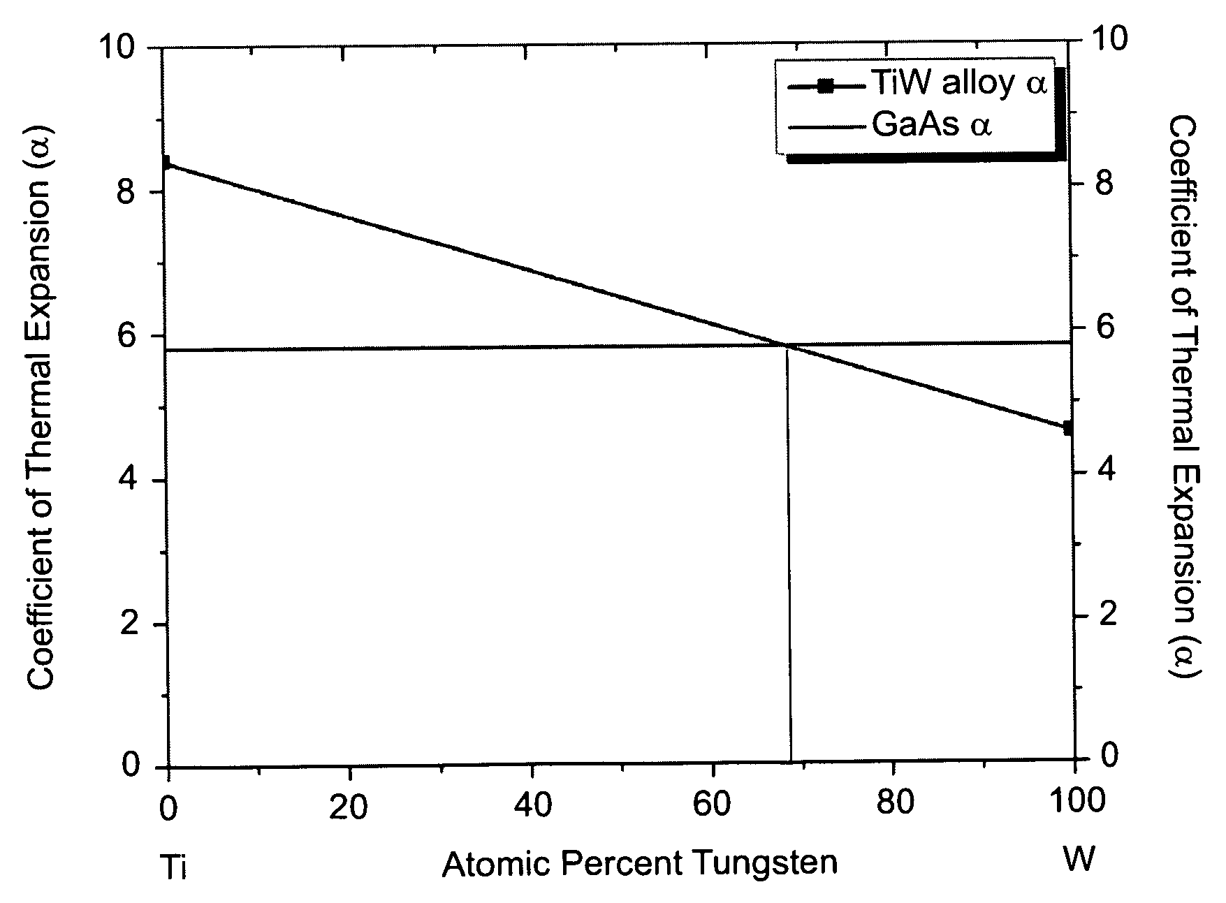
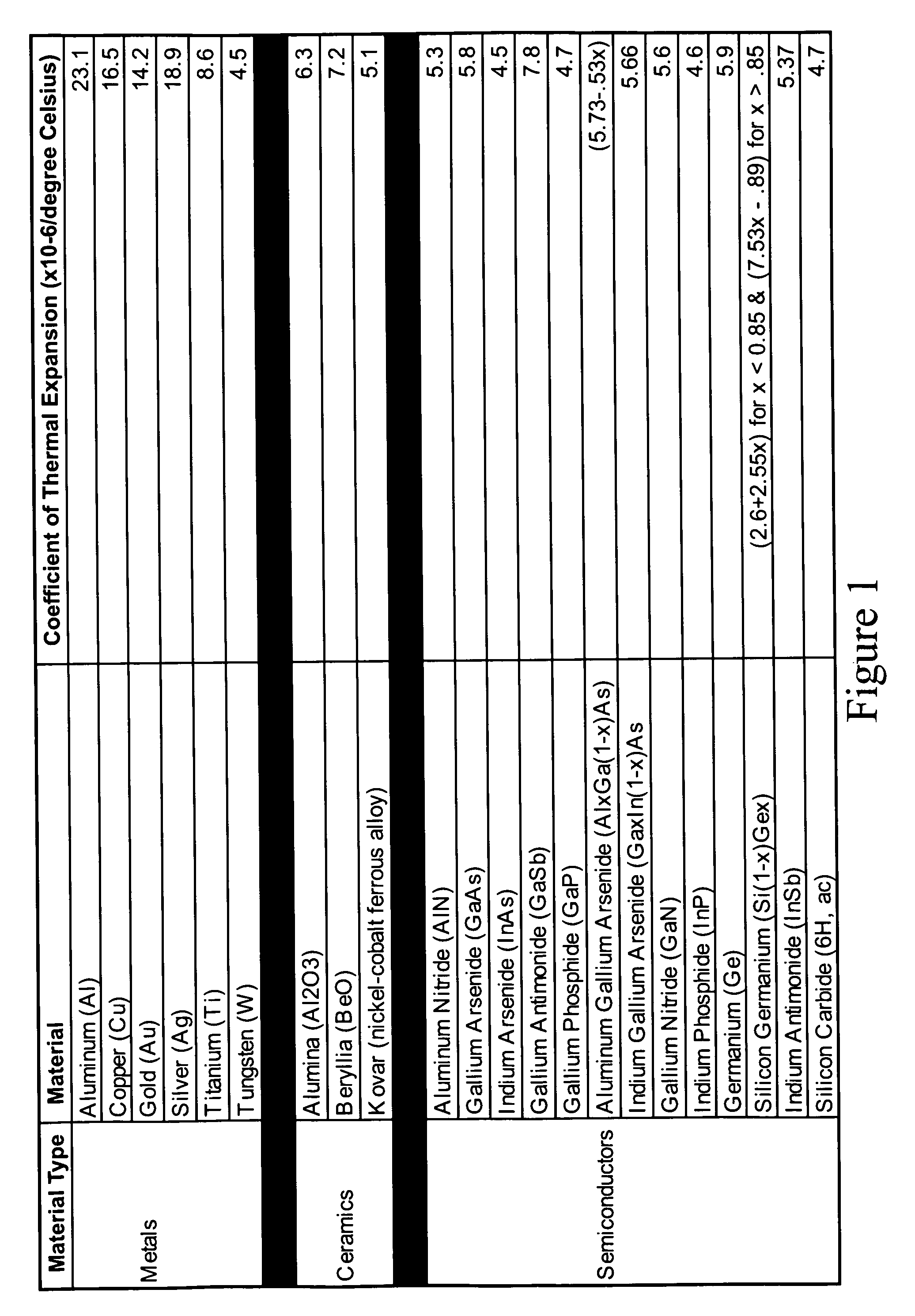
Specifically, any differences in the respective Coefficient of Thermal Expansion (CTE) between the semiconductor and the metal substrate can result in large “built-in” residual stresses that can have detrimental effects on the semiconductor device performance.
Metals usually have relatively large coefficients of thermal expansion, whereas semiconductors have comparatively lower coefficients of thermal expansion, and therefore, the differing thermal expansion coefficients of the materials in this system, combined with the elevated temperatures required to perform the soldering process, can result in large built-in stresses between the mated substrates once they are cooled to room temperature.
Additionally, most semiconductor devices heat up very significantly during operation and can result in thermal stresses and strains to develop between the semiconductor device and the metal substrate it is mounted to.
Specifically, this operational heating combined with the differing coefficients of thermal expansion results in a thermal stress and strain on the semiconductor devices.
These built-in stresses frequently result in many negative consequences for the performance of semiconductor device(s).
Furthermore, large built-in stresses have been known to appreciably lower the reliability of semiconductor devices.
For example, most semiconductor devices heat-up due to the power dissipated during operation thereby resulting in a thermal strain to develop between the mated materials.
Under some circumstances, this thermal strain can become sufficiently large so as to result in the fracture of the semiconductor substrate, thereby resulting in an inoperable semiconductor device(s).
Additionally, a sufficiently large thermal strain between a joined semiconductor and metal substrate can result in the substrates breaking apart due to a failure at the interface.
Moreover, even if the thermal strain is not sufficiently large to cause fracture in one operational cycle, fracture can still result after many operational cycles (e.g., power on for some period of time with a resultant increase in heating and thermal stain, followed by a period of time with the power off and a decrease in heating and thermal strain, followed by a period of time with power on again with a resultant increase in heating and thermal strain, etc.), due to fatigue effects in the semiconductor substrate over multiple cycles of operation.
Even in cases where fracture due to fatigue does not occur, the additional strain will lower the reliability of the solid-state semiconductor devices.
For example, a laser diode that is under a strain due to packaging or mounting stresses will have its bandgap in the semiconductor modified and this change in the bandgap may result in increased currents at certain locations in the device that, if sufficiently large, will overstress the material and eventually cause it to fail.
In the case of light emitting devices the additional strain will result in undesirable wavelength shifts, thereby decreasing the performance of the device.
Additionally, it is known that the thermal and mechanical stresses between semiconductor substrates mounted onto metal substrates can cause the solders used to join the metal and semiconductors substrates to re-flow from the interface to other areas of the device and / or package, which can result in a number of problems, such as the electrical shorting of the device.
In some instances, this solder may re-flow to locations that cause an electrical shorting between parts of the device meant to be electronically isolated thereby resulting in catastrophic failure of the device.
Solder re-flow may also result in the solder material encroaching and obstructing into sensitive locations of the device.
Alternatively, or in addition to these phenomena, the solder layer(s) used for joining metal to semiconductor substrates can re-flow away from the areas where electrical current is flowing and voltage potential is applied, thereby resulting in an open circuit condition, as well as other serious and negative effects on the semiconductor device(s).
If the solder re-flows from the interface between the metal and semiconductor substrates, the result could be the creation of voids at certain locations and an accompanying increase in the electrical resistance across the metal to semiconductor interface in locations where the solder is no longer present.
Moreover, in the locations where the solder has moved away from the interface, thereby forming voids in the electrical continuity at the metal to semiconductor junction, the re-flow process, if left to continue, can eventually result in an open-circuit condition of the device.
Furthermore, in the locations where the current is concentrated, the temperature of the interface will rise, thereby causing more solder to re-flow and consequently reinforcing the process to continue or even accelerate it, with the eventual result that the semiconductor device(s) fails to operate.
As a result, the temperature of the semiconductor device(s) will rise since the heat cannot be transferred as effectively away from the semiconductor substrate.
Consequently, a positive feedback process is established whereby the semiconductor device and substrate heating reinforces the solder migration, which causes additional temperature rise in the semiconductor, with the eventuality that the semiconductor fails to operate.
Even for semiconductor devices where the result is not catastrophic failure, overheating caused by solder re-flow can have very serious consequences for the reliability of the semiconductor device(s).
Therefore, it can be seen that as the temperature rises, the rate of failure increases exponentially.
Therefore, for some devices, even relatively small temperature increases (e.g., a few degrees Celsius), can result in a very large decrease in device reliability.
Therefore, any phenomena resulting in even a slight over-temperature of the semiconductor devices will have significant and negative effects on the semiconductor device reliability.
Even if other materials, such as adhesives, epoxies, glues, etc., are used to join or attach a semiconductor substrate to a metal substrate, there can be appreciable and undesired stresses in the semiconductor substrates partially or totally as a result of the large thermal expansion coefficient mis-match between most metallic materials and semiconductors.
Additionally, adhesives tend to shrink when they cure, which also can lead to significant stresses and strains in the semiconductor substrate and the associated increase in problems with reliability and failures.

Method used


Image

  • Tailorable titanium-tungsten alloy material thermally matched to semiconductor substrates and devices
  • Tailorable titanium-tungsten alloy material thermally matched to semiconductor substrates and devices
  • Tailorable titanium-tungsten alloy material thermally matched to semiconductor substrates and devices

Examples


Embodiment Construction

[0042]In many electronic, microelectronic, photonic, MEMS, MMIC, power electronics, NEMS, nanotechnology, thermoelectric and other similar applications of semiconductor devices in the commercial and military sectors, the semiconductor substrate into which the active device(s) are made is attached, joined, or bonded to a metallic substrate. There are a variety of benefits derived from mounting a semiconductor substrate on a metallic substrate, including: (1) metallic materials having high thermal conductivities, to thereby efficiently conduct heat away from the semiconductor substrate during operation by allowing the metallic substrate to function as a heat sink or heat spreader; (2) the high electrical conductivity of metallic materials that allows the metallic substrate to function as an electrode to the semiconductor substrate, thereby allowing current and voltage to be applied to the semiconductor device(s) to enable them to operate; and (3) the metal substrate providing mechanic...


PUM

PropertyMeasurementUnit
temperatureaaaaaaaaaa
coefficient of thermal expansionaaaaaaaaaa

Abstract

The present invention relates generally to a metallic alloy composed of Titanium and Tungsten that together form an alloy having a Coefficient of Thermal Expansion (CTE), wherein the content of the respective constituents can be adjusted so that the alloy material can be nearly perfectly matched to that of a commonly used semiconductor and ceramic materials. Moreover, alloys of Titanium-Tungsten have excellent electrical and thermal conductivities making them ideal material choices for many electrical, photonic, thermoelectric, MMIC, NEMS, nanotechnology, power electronics, MEMS, and packaging applications. The present invention describes a method for designing the TiW alloy so as to nearly perfectly match the coefficient of thermal expansion of a large number of different types of commonly used semiconductor and ceramic materials. The present invention also describes a number of useful configurations wherein the TiW material is made as well as how it can be shaped, formed and polished into heat sink, heat spreaders, and electrodes for many applications. The present invention also discloses the direct bonding of a TiW substrate to a semiconductor substrate.

Description

[0001]This application claims the benefit of Provisional Application No. 61 / 129,736, filed Jul. 15, 2008, the entire contents of which are hereby incorporated by reference in this application.FIELD OF THE INVENTION[0002]The present invention relates generally to a metallic alloy composed of Titanium and Tungsten that together form an alloy having a Coefficient of Thermal Expansion (CTE) that can be adjusted by adjusting the content of the constituent metals so that the CTE of the alloy metal nearly perfectly matches that of commonly used semiconductor and ceramic materials. Alloys of Titanium-Tungsten have excellent electrical and thermal conductivities making them ideal material choices for many electrical, photonic, packaging and MEMS applications.BACKGROUND OF THE INVENTION[0003]Metal and metal alloy materials are used in many semiconductor applications, including electronics, microelectronics, photonics, Micro-Electro-Mechanical Systems (MEMS), Nano-Electro-Mechanical Systems (N...

Claims


Application Information

Patent Timeline
Patent Type & Authority Patents(United States)
IPC IPC(8): C22C1/00C22C1/04H01L23/373H01L23/473H01S5/024H01S5/40
CPCC22C1/00H01L23/3736C22C1/045H01L23/473H01S5/02423H01S5/4025H01S5/02476H01L2224/48472H01L2224/32245H01L2224/73265H01L2924/1461H01L2224/48247H01L2924/3025H01L2224/48091H01L2924/00014H01L2924/00
Inventor HUFF, MICHAEL A.SUNAL, PAUL
Owner FOR NAT RES INITIATIVES
Why Eureka
Try Eureka