
Microfine structure formation method and microfine structure formed body

a microstructure and structure technology, applied in the field of microstructure formation methods and microstructure formation methods, can solve the problems of increasing the difficulty of processing such a microstructure by photolithography, and the increase in the exposure time (or drawing time) requires a longer time for completing the pattern

Active Publication Date: 2014-12-23
HITACHI-LG DATA STORAGE
View PDF3 Cites 0 Cited by
  • Summary
  • Abstract
  • Description
  • Claims
  • Application Information

AI Technical Summary

Benefits of technology

This method achieves a thinner and more uniform remaining film on the substrate, significantly increasing the number of repeatable transfer times while maintaining high accuracy and reducing defect rates, even at larger pattern sizes and aspect ratios.

Problems solved by technology

However, it has become difficult to process such a microfine pattern by the photolithography techniques, as the formation of extremely small patterns has progressed, and the required pattern dimension has nearly reached a wavelength of light used in an exposure process.
Therefore, there is a disadvantage in the electron beam writing method in which increase in an exposure time (or drawing time) requires a longer time for completing the pattern formation as the number of patterns to be drawn increases.
As a result, the higher a degree of integration of a semiconductor integrated circuit becomes, the longer a time required for the pattern formation increases, which raises concerns on reduction of the throughput.
However, the pattern formation by the batch graphic irradiation method has been resulted in inevitably large-sized apparatus of such an electron beam lithography apparatus and requirement for control in high accuracy of mask alignment.
This causes a disadvantage that the apparatus cost increases.
However, the mold-releasability of the stamper from the resin layer begins gradually deteriorating in proportion as the number of repeatable transfer times onto the resin layer increases.
The stamper with deteriorated mold-releasability gives rise to deterioration in the pattern to be transferred on the resin layer.
However, there is a drawback that the cost of the product obtained from the transferred pattern cannot be lowered enough, from a viewpoint of the number of the repeatable transfer times per one time treatment of the mold-releasing agent with maintaining the predetermined transferring quality.
Specifically, release of the stamper from the resin layer becomes more difficult, as the ratio of the aspect of the pattern becomes larger and the pattern size becomes smaller.
When the aspect ratio of the pattern becomes two or more, the convex parts of the transferred pattern in the resin layer are easy to collapse, and the resinous portion corresponding to the convex part is transferred to the stamper, causing a defect in the transferred pattern in the releasing process.
However, as disclosed in Japanese Unexamined Patent Application Publications No. 2012-41521 and No. 2009-158729, the conventional method for improving the mutual adhesion between the resin layer and the substrate has a disadvantage that the adhesion therebetween becomes insufficient when the thickness of the remaining layer becomes thin, which causes the remaining film to be transferred to the stamper.

Method used


Image

  • Microfine structure formation method and microfine structure formed body
  • Microfine structure formation method and microfine structure formed body
  • Microfine structure formation method and microfine structure formed body

Examples


example 1

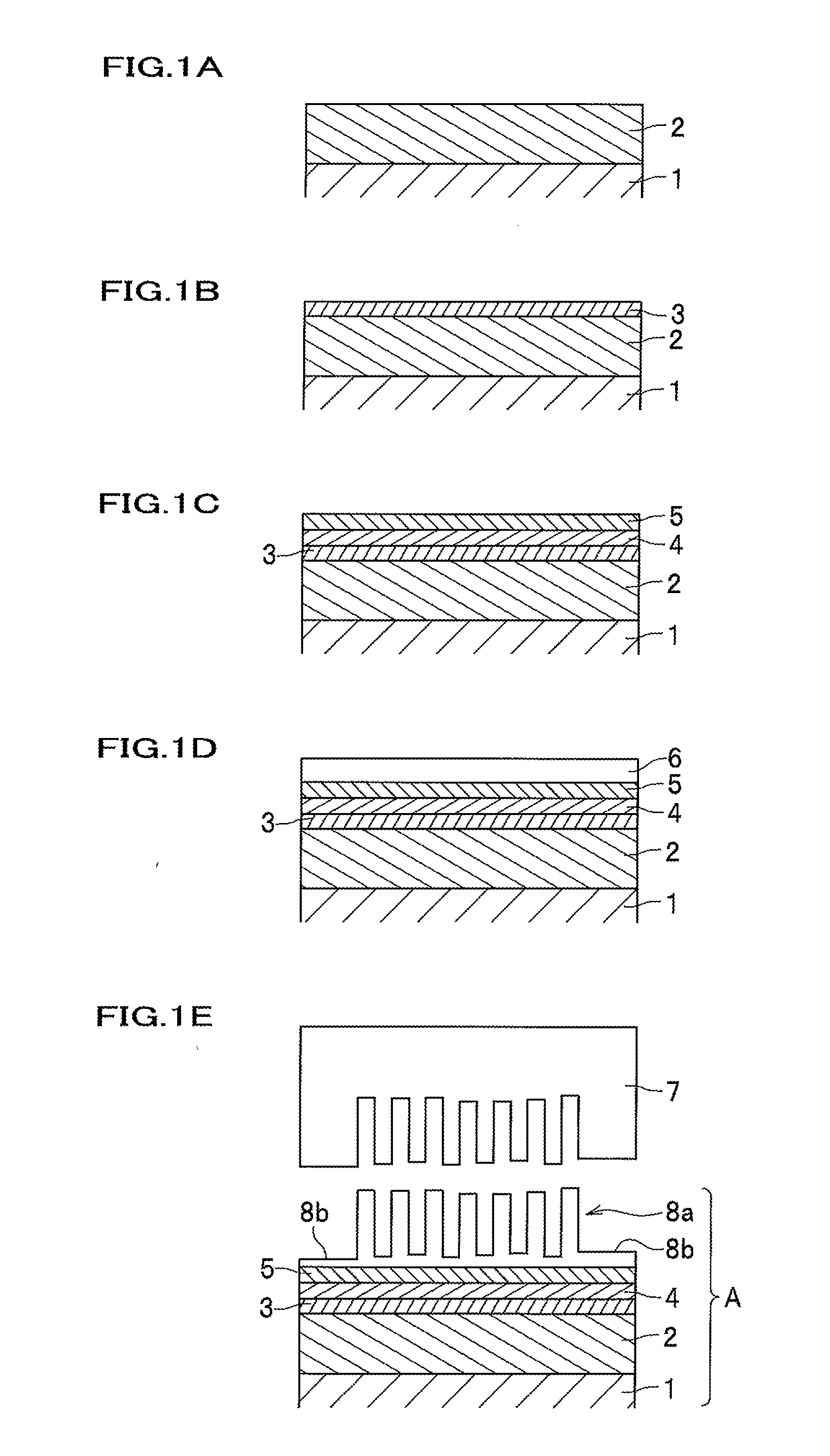
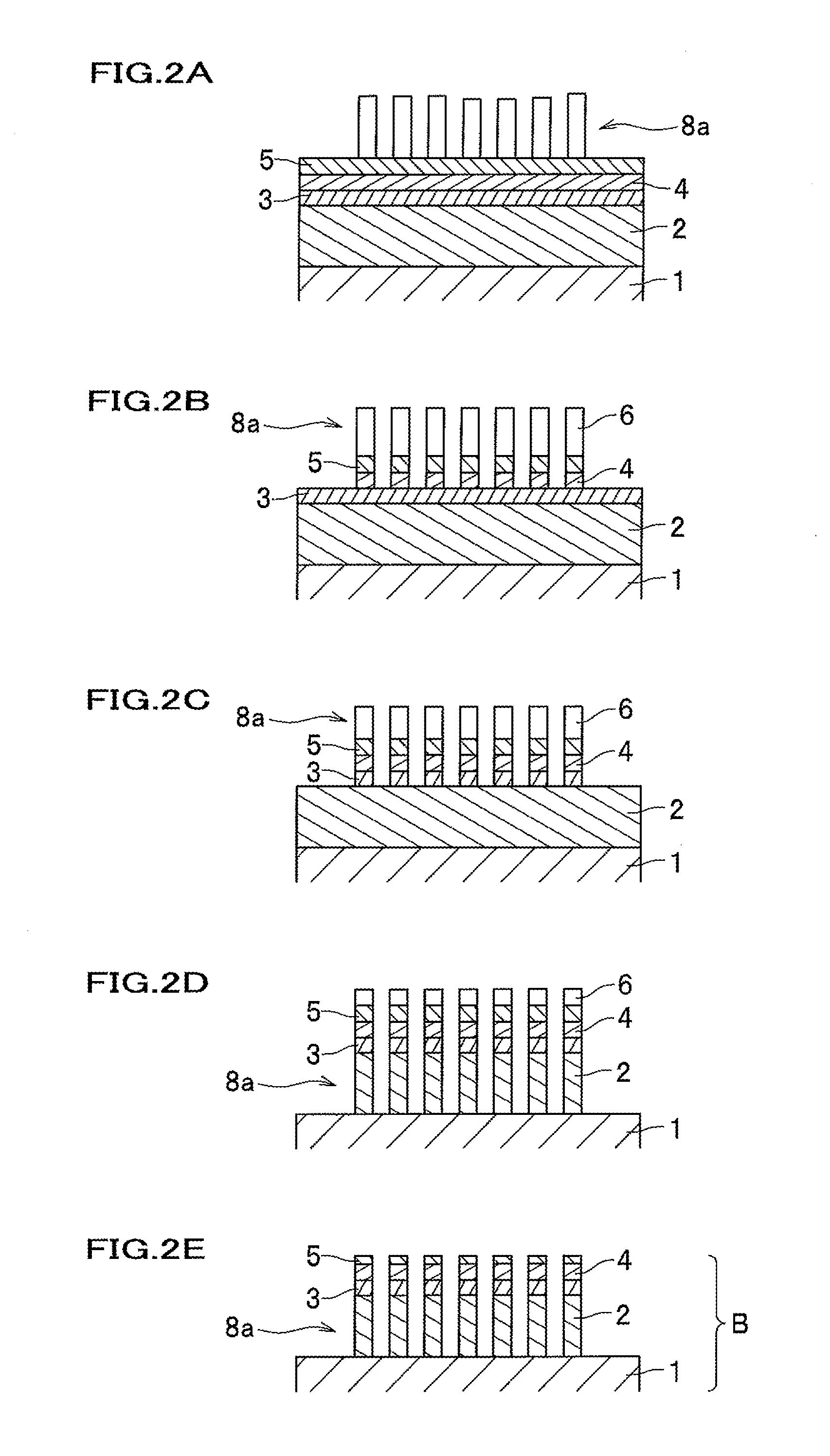
[0102]In this EXAMPLE 1, the microfine structure forming bodies A and B were prepared by performing the steps shown in FIGS. 1A to 1E and FIGS. 2A to 2E.

[0103]As shown in FIG. A, the metallic thin film 2 consisting of aluminum (thickness of 150 nm) was deposited on the surface of the substrate 1 (a synthetic quartz substrate: diameter of 100 mm, thickness of 0.7 mm) by a spattering method.

[0104]Next, as shown in FIG. 1B, the oxide layer 3 (thickness of 6 nm) was formed on the surface of the metallic thin film 2 by an O2 plasma treatment method.

[0105]As shown in FIG. 1C, the first adhesive layer 4 was first deposited on the surface of the oxide layer 3 by a vapor deposition method via using bis(triethoxysilylpropyl)-disulfide (Wako Pure Chemical Co. Ltd.). Next, on the surface of the first adhesive layer 4 thus obtained, the second adhesive layer 5 was deposited by a vapor deposition method via using γ-glycidoxypropyl-trimethoxysilane (Tokyo Chemical Industry Co., Ltd.)

[0106]Next, as...

example 2

[0124]In this EXAMPLE 2, bis-triethoxysilylethane (Tokyo Chemical Industries, Co. Ltd.) was used for the first adhesive layer 4, and 3-acryloylpropyltrimethoxysilane (Shin-etsu silicone Co. Ltd.) was used for the second adhesive layer 5, as shown in FIG. 1C.

[0125]Further, the photocurable resin layer 6 was formed by using an acrylate mixture of which main component was neopentylglycol diacrylate (Shin-Nakamura Chemical Industries Co. Ltd.).

[0126]Except for the above mentioned differences, totally 100 microfine structure forming bodies A and B were respectively prepared in the same method as in EXAMPLE 1.

[0127]The first microfine structure forming body A had a height of 84±2 nm at the pattern part (or convex part 8a) and a thickness of 7±3 nm at the remaining film part 8b. The first microfine structure forming body B had a full-pitch of 150±1 nm, a land-pitch of 88±5 nm, and a height of 150±1 nm. Within a circular area of a 100 mm diameter in the first microfine forming body structur...

example 3

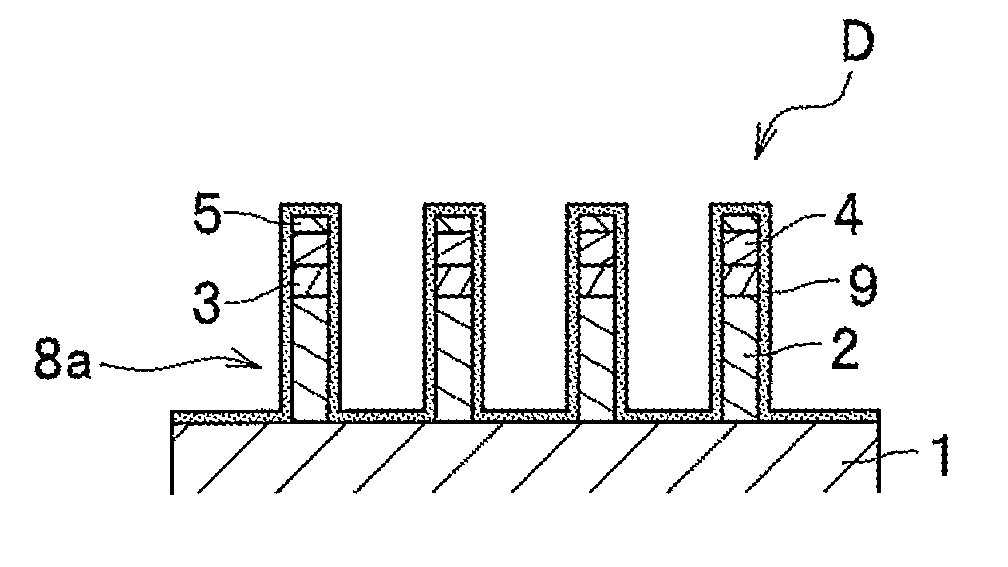
[0131]In this EXAMPLE 3, a microfine structure forming body C forming a microfine structure on the substrate 1 (shown in FIG. 3) was prepared by etching the microfine structure forming body B (refer to FIG. 2E) prepared in EXAMPLE. 1 using fluorine based gas.

[0132]A cross sectional surface of the microfine structure forming body C was measured at several points by a SEM (scanning electron microscope). Hereby, it was determined that a line-and-space pattern made of glass was formed, having a full pitch of 150±1 nm, a land pitch of 88±6 nm, and a height of 100±1 nm.

[0133]Note a defect rate of the line-and-space pattern within a circular area having a 100 mm diameter in the microfine structure forming body B was less than 1%.


PUM

PropertyMeasurementUnit
thicknessaaaaaaaaaa
thicknessaaaaaaaaaa
thicknessaaaaaaaaaa

Abstract

Provided are a method for forming a microfine structure and a microfine structure forming body prepared by the method. The method allows a remaining film part to be formed thinner and more uniform on a substrate than the conventional techniques. The method comprises the steps of: forming an oxide layer on a metallic thin film; a photocurable resin layer via first and second adhesive layers over the oxide layer; and transferring a microfine structure formed on a mold by pressing the mold onto the photocurable resin layer. The first adhesive layer includes a compound having at least two hydrolysable functional groups, and the second adhesive layer includes a compound having at least a hydrolysable functional group and a reactive functional group.

Description

CROSS REFERENCE TO RELATED APPLICATIONS[0001]This application claims the foreign priority benefit under Title 35, United State Code, 119 (a)-(d) of Japanese Patent Application No. 2013-028529, filed on Feb. 18, 2013 in the Japan Patent Office, the disclosure of which is herein incorporated by reference in its entirety.BACKGROUND OF THE INVENTION[0002]1. Field of the Invention[0003]The present invention relates to a method for forming a microfine structure comprising a metal on a substrate, and a microfine structure forming body formed by the method.[0004]2. Description of Related Art[0005]Recently, photolithography techniques have been used frequently for processing a microfine pattern required for semiconductor devices, etc. However, it has become difficult to process such a microfine pattern by the photolithography techniques, as the formation of extremely small patterns has progressed, and the required pattern dimension has nearly reached a wavelength of light used in an exposure...

Claims


Application Information

Patent Timeline
Patent Type & Authority Patents(United States)
IPC IPC(8): H01L21/308H01L29/06H01L21/311
CPCH01L29/0657H01L21/3086G03F7/0002G11B5/00H01L21/31144H01L21/3088G11B5/746G11B5/855G11B5/865G11B7/256G11B7/263
Inventor WASHIYA, RYUTAOGINO, MASAHIKONAGASHIMA, SHIROYABE, AKIOSUGITA, MASAKIMIYAUCHI, AKIHIRO
Owner HITACHI-LG DATA STORAGE
Learn More