
Patterning process

a technology of patterning and process, applied in the field of patterning process, can solve the problems of high cost of scanner, change of optical system, and extremely poor sustainability, and achieve the effect of high beam energy

Active Publication Date: 2015-03-31
SHIN ETSU CHEM CO LTD
View PDF40 Cites 3 Cited by
  • Summary
  • Abstract
  • Description
  • Claims
  • Application Information

AI Technical Summary

Benefits of technology

[0015]The present invention was made in view of the situation mentioned above, and has an object to provide a patterning process especially suitable for a fine patterning material to be used in manufacturing of a very large scale integrated circuit by obtaining a pattern having a microdomain structure formed by self-assembly with excellent uniformity and regularity, the pattern having been difficult to be obtained by a conventional block polymer.
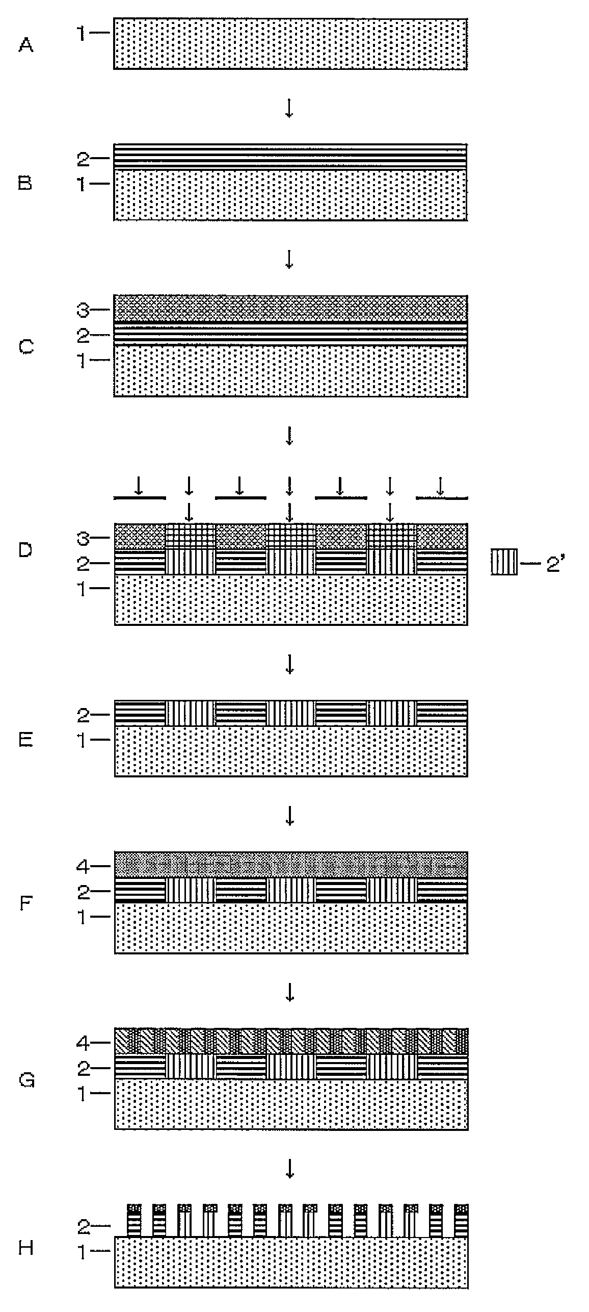
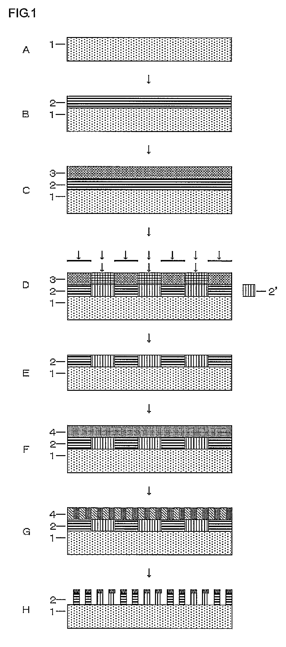
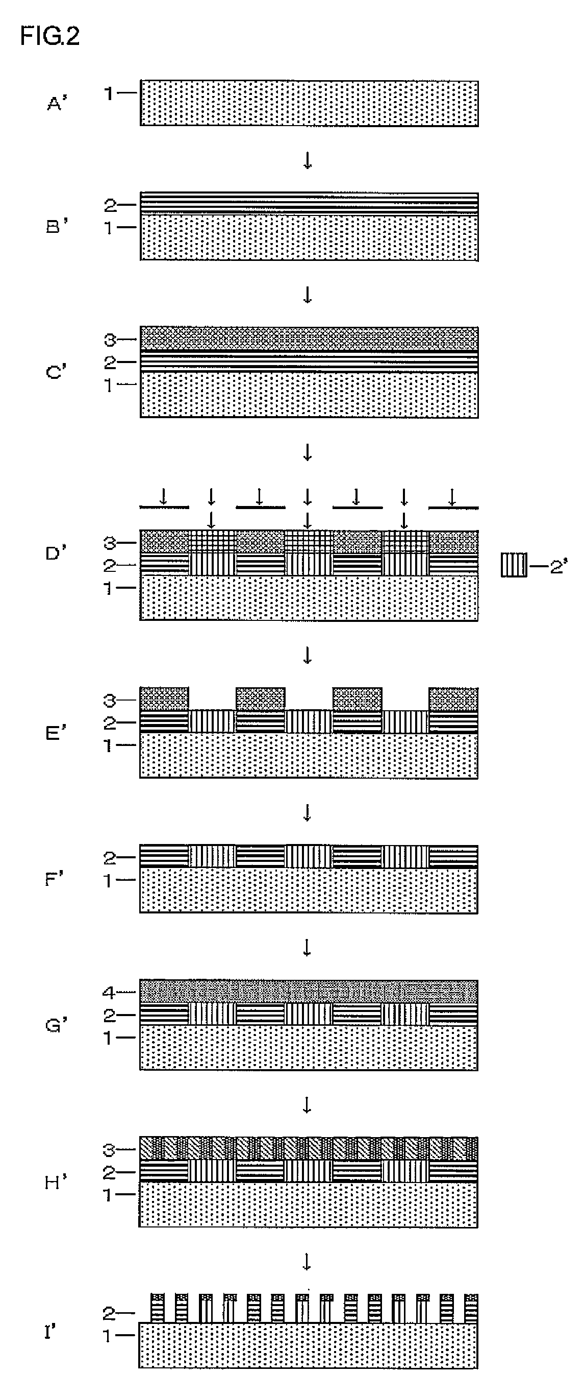
[0026]According to the patterning processed of the present invention, a pattern having a microdomain structure formed by self-assembly with excellent uniformity and regularity, the pattern having been difficult to be obtained by a conventional self-assembling polymer, can be obtained because this process includes the steps shown above; and thus, the present invention can provide a patterning process especially suitable for a fine patterning material to be used in manufacturing of a very large scale integrated circuit and the like.
[0030]By forming a CVD film or an organic underlayer film under the silicon-containing film used in the present invention and by optimizing a combination thereof with a film to be processed, a fine pattern by self-assembly can be transferred to an inorganic film and a semiconductor device substrate in a further lower layer without a difference in size conversion.
[0031]According to the patterning process of the present invention, self-assembly of the self-assembling polymer can be accelerated so that fine patterning that cannot be reached by a lithography using a high beam energy can be obtained and pattern transfer by using this film as an etching mask becomes possible.

Problems solved by technology

However, there are many problems with the F2 lithography: cost-up of a scanner due to use of a large quantities of expensive CaF2 single crystals for a projection lens; extremely poor sustainability of a soft pellicle, which leads to change of an optical system due to introduction of a hard pellicle; decrease in etching resistance of a photoresist film, and so forth.
Problems to be solved in the EUV lithography are to obtain a higher output power of the laser, a higher sensitivity of the photoresist film, a higher resolution power, a lower line edge roughness (LER), a non-defect MoSi laminate mask, a lower aberration of the reflective mirror, and so forth; and thus, there are mounting problems to be solved.
However, under the present situation, patterning to form a fine pattern by a lithography with 30 nm or less, especially by a lithography with 10 nm or less is difficult.
However, the pattern obtained by these self-assembly materials has many problems in uniformity and regularity of the pattern form even though the pattern thereof is about 30 nm in its size, so that this has not been realized as a practical method; and thus, these problems are required to be solved.

Method used


Image

  • Patterning process
  • Patterning process
  • Patterning process

Examples


synthesis example 1-1

[0160]Into a mixture of 220 g of methanol, 0.2 g of methanesulfonic acid, and 80 g of deionized water was added a mixture of 25.9 g of Monomer 101, 41.9 g of Monomer 102, and 9.5 g of Monomer 120; and then, they were kept at 40° C. for 12 hours to carry out the hydrolysis condensation reaction. After the reaction, 200 g of propylene glycol ethyl ether (PGEE) was added thereinto; and then, the by-produced alcohol was distilled out under reduced pressure. Then, 1000 mL of ethyl acetate and 300 g of PGEE were added thereinto to separate the water layer. To the remained organic layer was added 100 mL of ion-exchanged water; and then, the resulting mixture was stirred, settled, and separated into the layers. This operation was repeated for three times. The remained organic layer was concentrated under reduced pressure to obtain 330 g of PGEE solution containing the silicon-containing compound 1-1 (compound concentration of 10%). The polystyrene-equivalent molecular weight of this compoun...

synthesis example 1-17

[0162]Into a mixture of 400 g of ethanol, 5 g of 25% tetramethyl ammonium hydroxide, and 200 g of deionized water was added a mixture of 20.4 g of Monomer 101, 7.6 g of Monomer 102, and 95.5 g of Monomer 128; and then, they were kept at 40° C. for 4 hours to carry out the hydrolysis condensation reaction. After the reaction, 2 g of acetic acid was added thereinto for neutralization, and then, the by-produced alcohol was distilled out under reduced pressure. Then, 1200 mL of ethyl acetate and 400 g of PGEE were added thereinto to separate the water layer. To the remained organic layer was added 100 mL of ion-exchanged water; and then, the resulting mixture was stirred, settled, and separated into the layers. This operation was repeated for three times. The remained organic layer was concentrated under reduced pressure to obtain 410 g of PGEE solution containing the silicon-containing compound 1-17 (compound concentration of 20%). The polystyrene-equivalent molecular weight of this co...

synthesis example 1-25

[0164]Into a mixture of 120 g of methanol, 0.1 g of 70% nitric acid, and 60 g of deionized water was added a mixture of 5.0 g of Monomer 100, 3.4 g of Monomer 101, and 68.5 g of Monomer 102; and then, they were kept at 40° C. for 12 hours to carry out the hydrolysis condensation reaction. After the reaction, 300 g of PGEE was added thereinto; and then, the by-produced alcohol and excess water were distilled out under reduced pressure to obtain 310 g of PGEE solution containing the silicon-containing film composition 1-25 (polymer concentration of 10%). The polystyrene-equivalent molecular weight of this compound was measured to be Mw=2,200.

[0165]Synthesis Example 1-26 to Synthesis Example 1-30 were carried out by using the monomers shown in Table 1 under the conditions similar to those in Synthesis Example 1-25 to obtain each of the intended products.

[0166]

TABLE 1SynthesisExampleRaw materials for reactionMw1-1 [Monomer 101]: 25.9 g, [Monomer 102]: 41.9 g, [Monomer 120]: 9.5 g2,2001-...


PUM

PropertyMeasurementUnit
wavelengthaaaaaaaaaa
refractive indexaaaaaaaaaa

Abstract

A patterning process which uses self-assembly, including: forming a silicon-containing film by applying a silicon-containing film composition having an organic substituent group substituted with an acid labile group onto a substrate to be processed, forming a photoresist film onto the silicon-containing film, pattern-exposing of the photoresist film, removing the photoresist film, forming a polymer film by applying a self-assembling polymer onto the silicon-containing film, self-assembling the polymer film to form a microdomain structure, forming a pattern of the polymer film having the microdomain formed, transferring the pattern to the silicon-containing film by using the pattern formed on the polymer as a mask, and transferring the pattern to the substrate to be processed by using the pattern transferred to the silicon-containing film as a mask. There can be provided a pattern having a microdomain structure formed by self-assembly with uniformity and regularity.

Description

BACKGROUND OF THE INVENTION[0001]1. Field of the Invention[0002]The present invention relates to a patterning process using self-assembly.[0003]2. Description of the Related Art[0004]In 1980s, photo-exposure using a g-beam (436 nm) or an i-beam (365 nm) of a mercury lamp as a light source had been widely used in the resist patterning. As a means for further miniaturization, shifting to a shorter wavelength of the exposure light was assumed to be effective, so that, in mass production process after the DRAM (Dynamic Random Access Memory) with 64 megabits (processing dimension of 0.25 μm or less) in 1990s, a KrF excimer laser (248 nm), a shorter wavelength than the i-beam (365 nm), had been used in place of the i-beam as an exposure light source. However, in production of DRAMs with integration of 256 MB and 1 GB or higher which require further miniaturized process technologies (processing dimension of 0.2 μm or less), a light source with further short wavelength is required, and thus...

Claims


Application Information

Patent Timeline
Patent Type & Authority Patents(United States)
IPC IPC(8): B44C1/22B82Y10/00B82Y40/00G03F7/00G03F7/09
CPCB44C1/227G03F7/0002G03F7/09B82Y10/00B82Y40/00
Inventor OGIHARA, TSUTOMUHATAKEYAMA, JUN
Owner SHIN ETSU CHEM CO LTD
Learn More