
Method for producing high quality, ultra-thin organic-inorganic hybrid perovskite

a technology of organic and organic inorganic perovskite, which is applied in the manufacture of electrolytic capacitors, sustainable manufacturing/processing, and final product manufacturing. it can solve the problems of reducing the overall transparency of the device stack, limiting the processibility of all low-temperature solution technology, and preventing the applicability of flexible plastic devices. , to achieve the effect of high-efficiency devices

Active Publication Date: 2017-10-17
THE UNITED STATES OF AMERICA AS REPRESETNED BY THE SEC OF THE AIR FORCE
View PDF8 Cites 22 Cited by
  • Summary
  • Abstract
  • Description
  • Claims
  • Application Information

AI Technical Summary

Benefits of technology

The present invention is overcoming issues in manufacturing thin perovskite films by providing a method for making a layered perovskite structure that is pinhole-free, continuous, and semitransparent. The method involves performing a surface treatment of a substrate with a passivating agent, applying a layer of PbI2, exposing it to methylammonium iodide in an orthogonal solvent, and annealing it. This resulted in a high-quality perovskite film with improved efficiency that can be used in various applications. The invention also provides alternatives, modifications, and equivalents within the scope of the present invention.

Problems solved by technology

However, the use of thick (≈200 nm) organic hole-transport layer leads to parasitic absorption losses, and thereby, reduces the overall transparency of the device stack.
Also, the fabrication of this type of device layout involves high temperature (>400° C.) sintering step for metal-oxides, which limits the technology's true benefit of all low-temperature solution processibility, and preclude its applicability to flexible plastic based devices.

Method used


Image

  • Method for producing high quality, ultra-thin organic-inorganic hybrid perovskite
  • Method for producing high quality, ultra-thin organic-inorganic hybrid perovskite
  • Method for producing high quality, ultra-thin organic-inorganic hybrid perovskite

Examples


examples

[0048]Procedure

[0049]Device Fabrication: All thin-film perovskite solar cell devices were fabricated on patterned indium-doped tin oxide (ITO) glass (Sheet resistance of 15Ω / □) substrates the day of deposition, the ITO glass substrates were cleaned sequentially by sonicating with detergent, deionized water, acetone, and isopropanol, followed by drying with a high flow of nitrogen and UV-ozone treatment for 20 min. Filtered (0.45 micron PVDF filter) poly-(3,4-ethylenedioxythiophene:poly(styrenesulfonic acid) (PEDOT:PSS; Clevios P from Heraeus Materials Technology) was spin coated onto the clean ITO glass substrates at 3000 rpm for 60 s and then dried on a ceramic hot-plate at 160° C. for 15 min in ambient atmosphere. Thereafter, the PEDOT:PSS coated ITO glass substrates were immediately taken into a nitrogen filled glove box (O2 level 2O level 3NH3PbI3 active layer was fabricated by a two-step sequential deposition method. First, hot PbI2 (dissolved in anhydrous dimethylformamide at ...


PUM

PropertyMeasurementUnit
charge carrier diffusion lengthaaaaaaaaaa
band gapsaaaaaaaaaa
absorption coefficientaaaaaaaaaa

Abstract

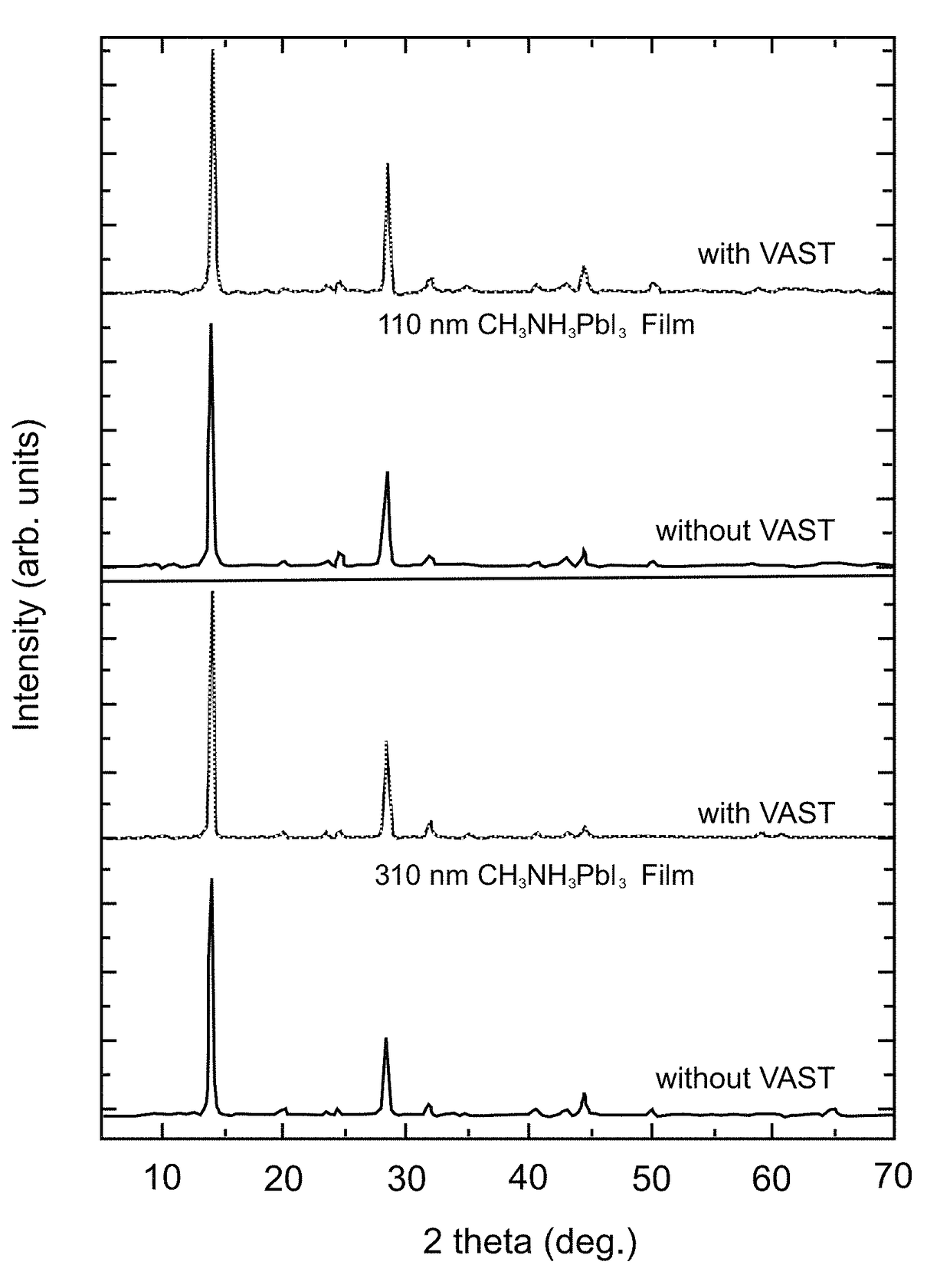
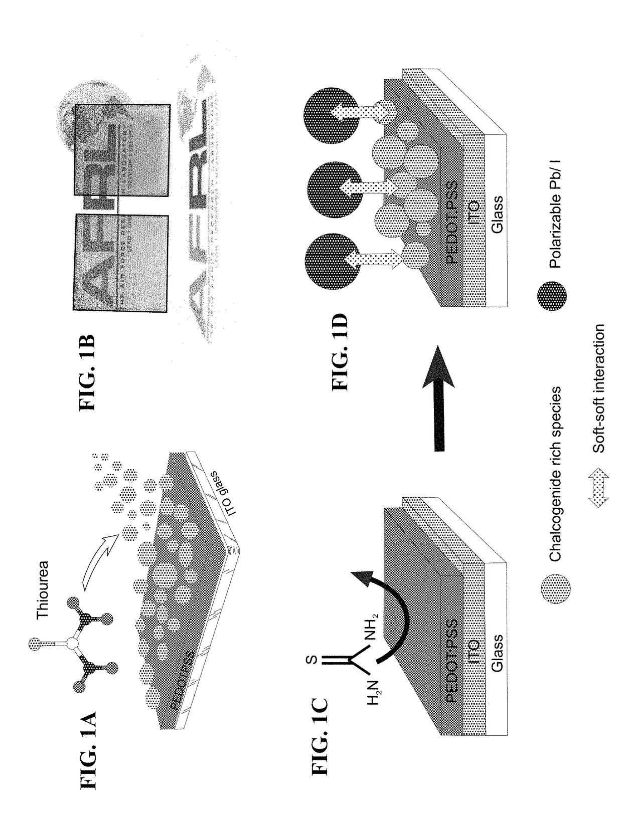
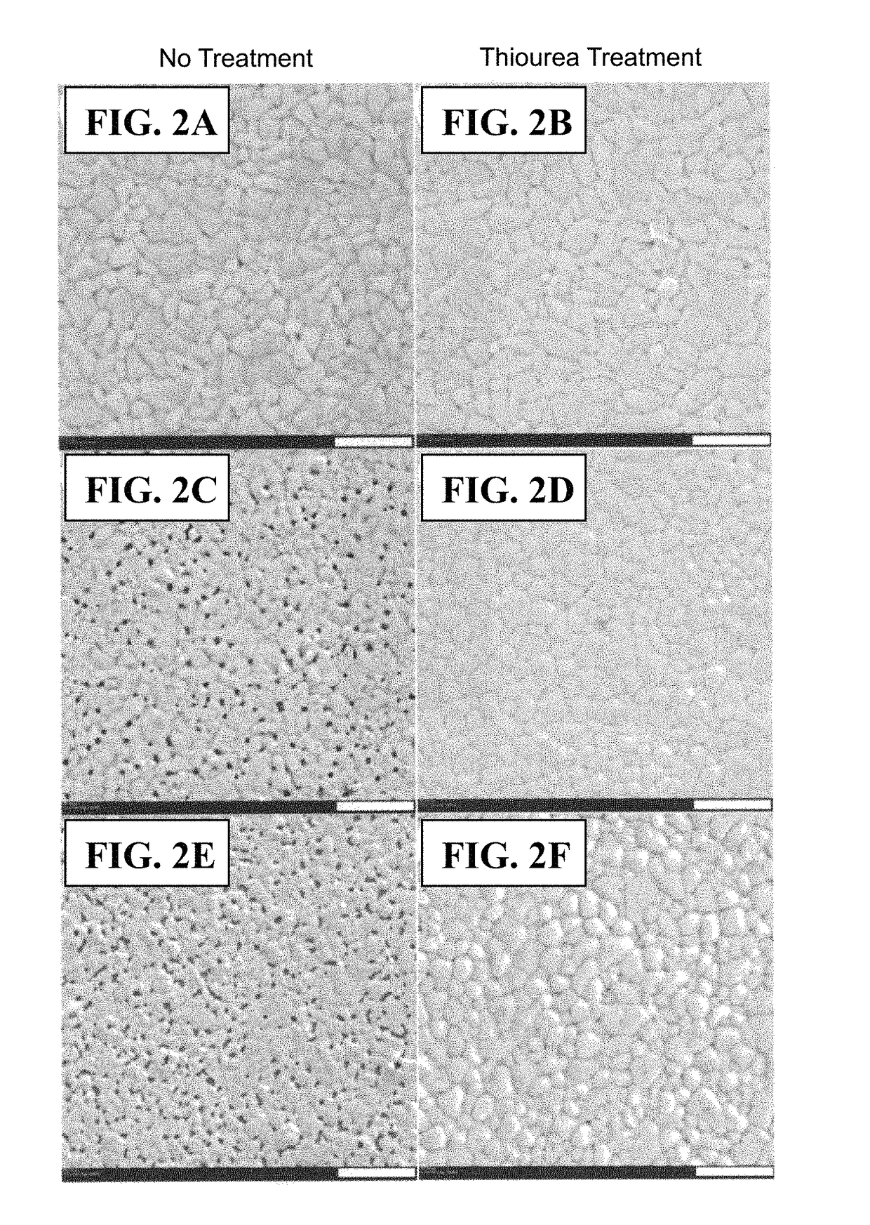
A method for making a layered perovskite structure comprises: a) performing a vapor assisted surface treatment (VAST) of a substrate with a surface passivating agent; b) applying a layer of PbI2 to the passivating agent; c) exposing the PbI2 to methylammonium iodide (CH3NH3I) in an orthogonal solvent; and d) annealing the structure. A PEDOT:PSS coated ITO glass substrate may be used. The surface passivation agent may be one a chalcogenide-containing species with the general chemical formula (E3E4)N(E1E2)N′C═X where any one of E1, E2, E3 and E4 is independently selected from C1-C15 organic substituents comprising from 0 to 15 heteroatoms or hydrogen, and X is S, Se or Te, thiourea, thioacetamide, selenoacetamide, selenourea, H2S, H2Se, H2Te or LXH wherein L is a Cn organic substituent comprising heteroatoms and X═S, Se, or Te. The passivating agent may be applied by spin-coating, inkjet-printing, slot-die-coating, aerosol-jet printing, PVD, CVD, and electrochemical deposition.

Description

RIGHTS OF THE GOVERNMENT[0001]The invention described herein may be manufactured and used by or for the Government of the United States for all governmental purposes without the payment of any royalty.FIELD OF THE INVENTION[0002]The present invention relates generally to hybrid organic-inorganic lead perovskites and, more particularly, to a method to produce high quality, ultra-thin organic-inorganic hybrid perovskite.BACKGROUND OF THE INVENTION[0003]A semitransparent photovoltaic (PV) device, in a variety of form factors, can address a range of applications outside the scope of traditional PV modules. Examples include building-integrated photovoltaics, photovoltaic curtains, self-powered green-houses, and wearable electronics. Solution-processable organic and dye-sensitized solar cells (OPV and DSSC, respectively) were studied for this purpose over the past several years due to their potential for low-cost, roll-to-roll compatible manufacturing process, light weight, mechanical fle...

Claims


Application Information

Patent Timeline
Patent Type & Authority Patents(United States)
IPC IPC(8): H01G9/00H01L31/072H01G9/20H01L51/42H01L51/00H01L31/0256
CPCH01G9/0029H01L51/42H01L51/0028H01L51/4213H01G9/2013H01L31/072H01L51/0077H01L2031/0344Y02E10/549Y02E10/542Y02P70/50H10K71/12H10K71/441H10K85/1135H10K85/30H10K30/20H10K85/50H10K30/50H10K2102/103
Inventor BAG, SANTANUDURSTOCK, MICHAEL F
Owner THE UNITED STATES OF AMERICA AS REPRESETNED BY THE SEC OF THE AIR FORCE
Learn More