Organic thin film transistor, organic semiconductor thin film, and organic semiconductor material

a thin film transistor and organic semiconductor technology, applied in the direction of non-metal conductors, conductors, organic chemistry, etc., can solve the problems of large change in threshold voltage in repeated driving, poor chemical stability, and inability to obtain good transistor characteristics immediately, etc., to achieve excellent chemical stability, high carrier mobility, and high carrier mobility

Inactive Publication Date: 2018-04-24
FUJIFILM CORP
View PDF10 Cites 0 Cited by
  • Summary
  • Abstract
  • Description
  • Claims
  • Application Information

AI Technical Summary

Benefits of technology

[0067]JP-A-2012-513459 does not describe a compound that has the same skeleton as the compound represented by the formula (1), but describes a structural isomer of the compound represented by the formula (1). However, the structural isomer has a low carrier mobility. WO 2010 / 114264 describes a compound that has the same skeleton as the compound represented by the formula (1), but the substituent on the N atom of carbazole has high bulkiness, and the compound has a low carrier mobility due to an insufficient overlap of electron orbitals with the adjacent molecule. In the invention, on the other hand, the advantageous effects of the invention may be obtained by using, as an organic semiconductor material, the compound that has a skeleton represented by the formula (1), has a bulkiness of the substituent on the N atom of carbazole that is reduced to such an extent that provides a sufficient overlap of electron orbitals with the adjacent molecule, and has the particular substituent introduced to the carbon atom constituting the ring of the dibenzocarbazole skeleton.
[0068]Preferred embodiments of the compound of the invention, the organic thin film transistor of the invention, and the like will be described below.Compound Represented by Formula (1)
[0069]The compound of the invention is represented by the following formula (1). The compound of the invention is contained in a semiconductor active layer described later in the organic thin film transistor of the invention. Thus, the compound of the invention may be used as a material for an organic thin film transistor.
[0070]wherein in the formula (1), Z represents a substituent that has a length of 3.7 Å or less from the N atom to the end of the substituent; and R1 to R8 each independently represent a hydrogen atom or a substituent, provided that at least one of R1 to R8 represents a substituent represented by the following formula (W):-L-R  Formula (W)wherein in the formula (W), L represents a divalent linking group represented by any one of the following formulae (L-1) to (L-12), or a divalent linking group containing 2 or more divalent linking groups each represented by any one of the following formulae (L-1) to (L-12) bonded to each other; and R represents a substituted or unsubstituted alkyl group having 2 or more carbon atoms, an oligooxyethylene group having a repeating number of an oxyethylene unit of 2 or more, or an oligosiloxane group having 2 or more silicon atoms:
[0071]wherein in the formulae (L-1) to (L-12), the wavy line represents a position bonded to the dibenzocarbazole skeleton, and * represents a position bonded to R in the formula (W); in the formula (L-1), n represents an integer of 1 or more; in the formula (L-10), m represents 4; in the formulae (L-11) and (L-12), m represents 2; and in the formulae (L-1), (L-2), (L-10), (L-11) and (L-12), R′ each independently represent a hydrogen atom or a substituent.
[0072]In the formula (1), Z represents a substituent that has a length of 3.7 Å or less from the N atom to the end of the substituent. The molecular length of the substituent Z herein means the length of from the N atom in the N—Z bond in carbazole of the dibenzocarbazole structure to the end of the substituent represented by Z. The structure optimization calculation may be performed by the density functional approach (Gaussian 03 (Gaussian, Inc., U.S.), base function: 6-31G*, exchange correlation function: B3LYP / LANL2DZ). In the formula (1), Z preferably represents a substituent that has a length of from 1.0 to 3.7 Å from the N atom to the end of the substituent, and more preferably a substituent that has a length of from 1.0 to 2.1 Å. The molecular lengths of representative substituents are 4.6 Å for a propyl group, 4.6 Å for a pyrrol group, 4.5 Å for a propynyl group, 4.6 Å for propenyl group, 4.5 Å for an ethoxy group, 3.7 Å for a methylthio group, 3.4 Å for an ethenyl group, 3.5 Å for an ethyl group, 3.6 Å for an ethynyl group, 3.3 Å for a methoxy group, 2.1 Å for a methyl group, and 1.0 Å for a hydrogen atom.

Problems solved by technology

However, it may not be said that a compound that is useful as a material for an organic EL device is immediately useful as a semiconductor material for an organic thin film transistor.
In general, an organic compound having high crystallinity may be a cause of light emission defects, such as in-plane electric field unevenness, in-plane light emission unevenness and light emission quenching, and thus the material for an organic EL device is demanded to have high amorphous property with low crystallinity.
Accordingly, even when an organic compound constituting a material for an organic EL device is diverted to an organic semiconductor material, good transistor characteristics may not immediately obtained.
Actually, the present inventors actually apply the polycyclic condensed compound in Patent Document 2 having an aromatic heterocyclic ring applied to an organic EL device to an organic thin film transistor, but it has been found that there is a problem that sufficient transistor characteristics are not obtained.
Furthermore, the investigations made by the inventors reveal that the change in the threshold voltage becomes large in repeated driving.
The large change in the threshold voltage brings about a problem that the transistor is deteriorated in reliability and may not be used for a prolonged period of time.
The change in the threshold voltage after repeated driving is a problem that has not been known in the art.
Patent Document 3 describes the carbazole having two benzo-condensed rings, but Patent Document 3 does not describe an example of the application of the compound described therein to an organic transistor, and the use of the compounds described therein has failed to provide sufficient transistor characteristics (a low carrier mobility).

Method used


Image

  • Organic thin film transistor, organic semiconductor thin film, and organic semiconductor material
  • Organic thin film transistor, organic semiconductor thin film, and organic semiconductor material
  • Organic thin film transistor, organic semiconductor thin film, and organic semiconductor material

Examples


example 1

Synthesis Example 1

Synthesis of Compound 5

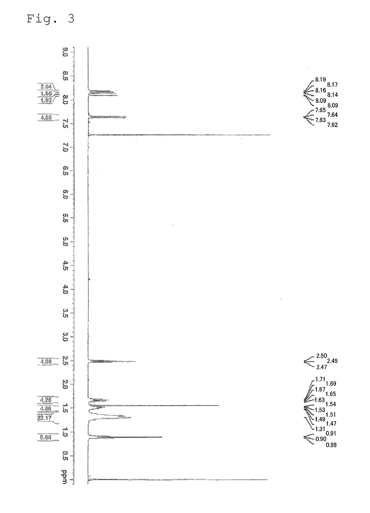
[0175]The compound 5 as the compound represented by the formula (1) was synthesized by the specific synthesis procedures shown by the following scheme. In the following scheme, Tf represents a trifluoromethanesulfonyl group (a triflyl group).

[0176]

Synthesis of Compound 5a

[0177]0.5 mL of concentrated hydrochloric acid was added to 3,4-dihydro-6-methoxynaphthalen-1(2H)-one (25 g) (produced by Wako Pure Chemical Industries, Ltd.) and an ethanol solution (120 mL) of hydrazine monohydrate (4.8 g), and the mixture was stirred under heating to reflux for 4 hours. The solid matter thus deposited was collected by filtration, rinsed with ethanol, and then dried under reduced pressure to provide a compound 5a (18.6 g).

Synthesis of Compound 5b

[0178]HCl-containing acetic acid (60 mL) (produced by Sigma-Aldrich Corporation) and acetic anhydride (6 mL) were stirred in a nitrogen atmosphere at 60° C. for 2 hours, to which the compound 5a (15 g) was added, a...

example 2

Formation of Semiconductor Active Layer (Organic Semiconductor Layer) Only with Compound

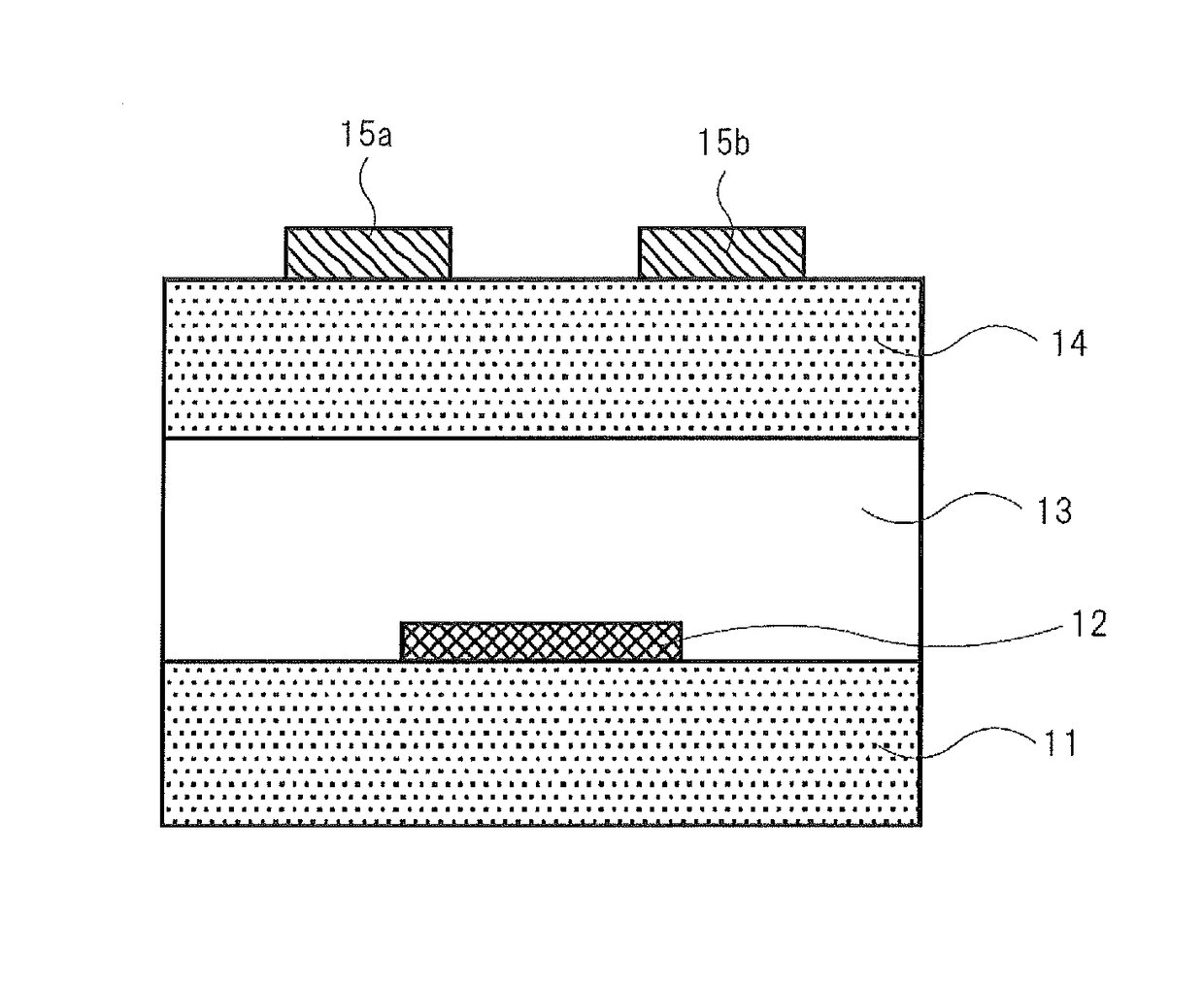
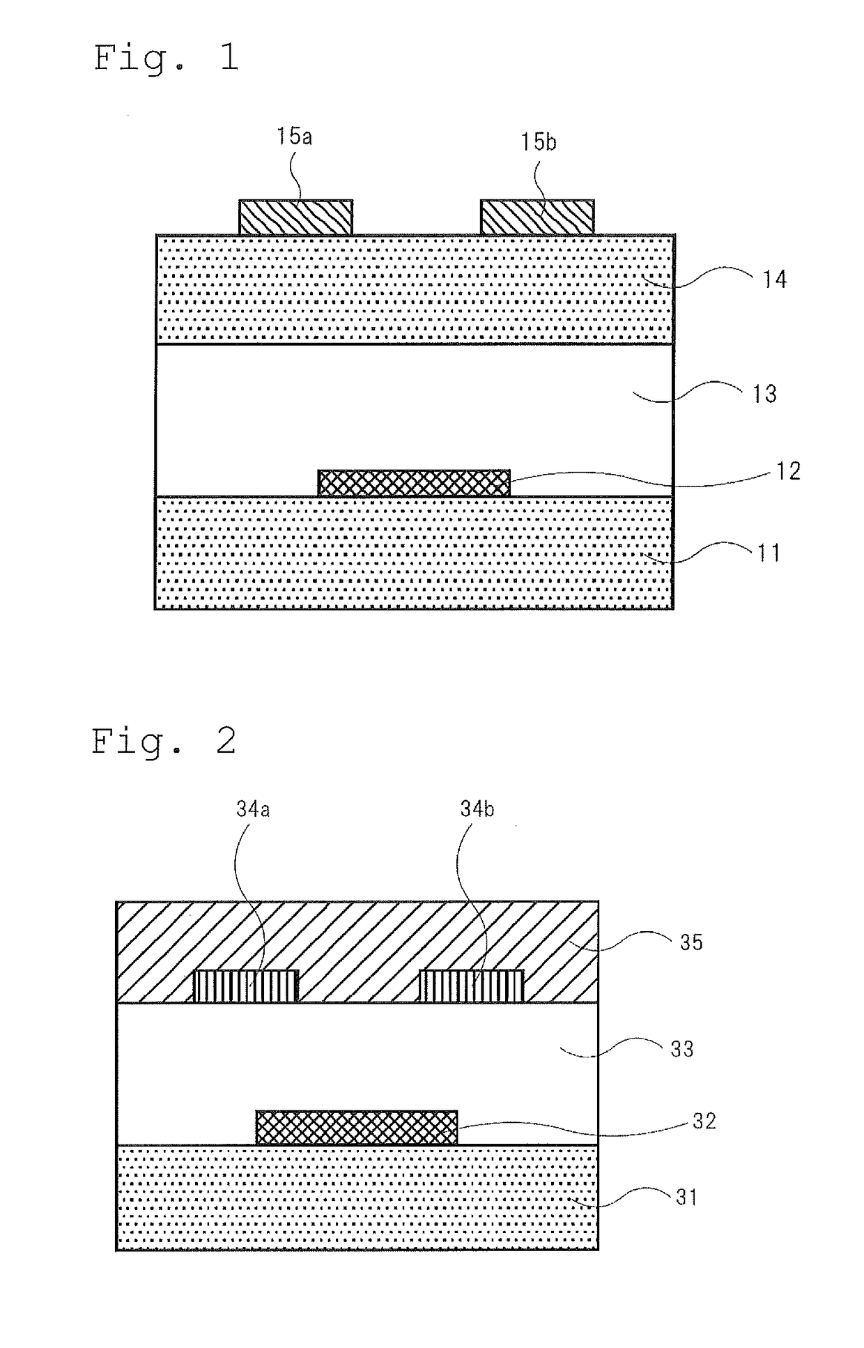
[0193]The compound of the invention or the comparative compound (1 mg each) and toluene (1 mL) were mixed and heated to 100° C. to prepare a coating solution for a non-light emitting organic semiconductor device. The coating solution was cast on a substrate for measuring FET characteristics heated to 90° C. to form an organic semiconductor thin film for a non-light emitting organic semiconductor device, thereby providing an organic thin film transistor device of Example 2 for measuring FET characteristics. The substrate for measuring FET characteristics used was a silicon substrate having a bottom-gate bottom-contact structure having chromium / gold electrodes (gate width W=100 mm, gate length L=100 μm) disposed in an interdigitated form as source and drain electrodes, and SiO2 (thickness: 200 nm) as an insulating film (the schematic structural illustration shown in FIG. 2).

[0194]The FET characteri...

example 3

Formation of Semiconductor Active Layer (Organic Semiconductor Layer) with Both Compound and Binder

[0202]Organic thin film transistor devices for measuring FET characteristics were produced in the same manner as in Example 2 except for using a coating solution prepared in such a manner that the compound of the invention or the comparative compound (1 mg each), 1 mg of PαMS (poly(α-methylstyrene), Mw: 300,000, produced by Sigma-Aldrich, Inc.) and toluene (1 mL) were mixed and heated to 100° C., and then evaluated in the same manner as in Example 2.

[0203]The results obtained are shown in Table 2 below.

[0204]

TABLE 2Change inthresholdOrganicCarriervoltage aftersemiconductormobilityrepeatedDevice No.material(cm2 / Vs)drivingNoteDevice 17Compound 11 × 10−1AinventionDevice 18Compound 53 × 10−1AinventionDevice 19Compound 84 × 10−1AinventionDevice 20Compound 106 × 10−2AinventionDevice 21Compound 113 × 10−1AinventionDevice 22Compound 131 × 10−1AinventionDevice 23Compound 145 × 10−3AinventionDev...


PUM

PropertyMeasurementUnit
thicknessaaaaaaaaaa
thicknessaaaaaaaaaa
thicknessaaaaaaaaaa

Abstract

An organic thin film transistor containing a compound represented by the following formula in a semiconductor active layer has a high carrier mobility and a small change in the threshold voltage after repeated driving. Z represents a substituent having a length of 3.7 Å or less, and at least one of R1 to R8 represents -L-R wherein L represents alkylene, etc., and R represents alkyl, etc.

Description

CROSS-REFERENCE TO RELATED APPLICATIONS[0001]This application is a Continuation of PCT International Application No. PCT / JP2014 / 052217 filed on Jan. 31, 2014, which claims priority under 35 U.S.C. Section 119(a) to Japanese Patent Application No. 2013-017018 filed on Jan. 31, 2013, and Japanese Patent Application No. 2014-015379 filed on Jan. 30, 2014. Each of the above applications is hereby expressly incorporated by reference, in its entirety, into the present application.BACKGROUND OF THE INVENTION[0002]Field of the Invention[0003]The present invention relates to an organic thin film transistor, an organic semiconductor thin film, and an organic semiconductor material. More specifically, the invention relates to a compound having a dibenzocarbazole structure, an organic thin film transistor containing the compound, an organic semiconductor material for a non-light emitting organic semiconductor device containing the compound, a material for an organic thin film transistor contain...

Claims


Application Information

Patent Timeline
Patent Type & Authority Patents(United States)
IPC IPC(8): H01L51/00C07D409/04C07D409/14C07D209/80H01B1/00H01B1/12H01L51/05
CPCH01L51/0072C07D209/80C07D409/04C07D409/14H01L51/0065H01L51/0067H01L51/0068H01B1/121H01L51/0558H01L51/0545H10K85/653H10K85/655H10K85/654H10K10/484H10K10/466H10K85/6572
Inventor TAKAKU, KOJIHIRAI, YUKISOTOYAMA, WATARUKINOSHITA, MASARU
Owner FUJIFILM CORP
Why Eureka
Try Eureka