Process for PECVD of silicon oxide using TEOS decomposition

a technology of pecvd and silicon oxide, which is applied in the direction of chemical vapor deposition coating, coating, plasma technique, etc., can solve the problems of increasing stringent requirements, increasing the difficulty of fabricating the conformal, planar inter-layer materials required, and reducing the efficiency of the process. , to achieve the effect of effective purging and preventing the breakdown of gas

Inactive Publication Date: 2000-03-21
APPLIED MATERIALS INC
View PDF15 Cites 82 Cited by
  • Summary
  • Abstract
  • Description
  • Claims
  • Application Information

AI Technical Summary

Benefits of technology

Preferably, a second, purge gas manifold is positioned beneath the wafer processing area for providing purging gas flow across the window and upward and across the bottom of the wafer. The combination of the high pressure, the purge flow from the inlet gas manifold and that from the purge gas manifold substantially eliminates deposition on chamber surfaces.
In still another aspect, the reactor of the present invention comprises a deposition gas feed-through device connected to the gas inlet manifold which comprises tube means adapted for providing co-axial flow of deposition gas on the inside of the tube and purge gas on the outside thereof into the gas inlet manifold. The tube is adapted for connection to ground at the inlet end and to an RF power supply at the outlet or manifold end to provide RF power to the manifold, and has a controlled electrical impedance along its length from the inlet to the outlet end for establishing a constant voltage gradient to prevent breakdown of the gas even at high RF frequencies and voltages.
These and other features discussed below permit reactor operation over a wide pressure regime, that is, over a wide of pressures including high pressures up to approximately one atmosphere. The features also provide uniform susceptor and wafer temperatures, including both absolute temperature uniformity and spatial uniformity across the susceptor / wafer; uniform gas flow distribution across the wafer; and effective purging. The variable parallel close spacing between the electrodes adapts the reactor to various processes. These features and the temperature control of the internal and external gas manifold temperatures enable the advantageous use of very sensitive unstable gases such as ozone and TEOS in processes such as the following.

Problems solved by technology

However, the deposition rates available using conventional plasma-enhanced processes are still relatively low.
However, single-wafer reactors have certain advantages, such as the lack of within-batch uniformity problems, which make such reactors attractive, particularly for large, expensive wafers such as 5-8 inch diameter wafers.
However, the incorporation into IC chips of, first, increasingly complex devices and circuits and, second, greater device densities and smaller minimum feature sizes and smaller separations, imposes increasingly stringent requirements on the basic integrated circuit fabrication steps of masking, film formation, doping and etching.
The increasing complexity, thickness / depth and small size of such multiple interconnect levels make it increasingly difficult to fabricate the required conformal, planar interlevel dielectric layers materials such as silicon dioxide that support and electrically isolate such metal interconnect layers.
Increasing the pressure used in the deposition process typically will increase the collision rate of the active species and decrease the mean-free path.
It is difficult to form conformal metal and / or dielectric layers over such topographies As a consequence, it is necessary to separately planarize the topography.

Method used


Image

  • Process for PECVD of silicon oxide using TEOS decomposition
  • Process for PECVD of silicon oxide using TEOS decomposition
  • Process for PECVD of silicon oxide using TEOS decomposition

Examples


Embodiment Construction

I. CVD / PECVD Reactor

A. Overview of CVD / PECVD Reactor

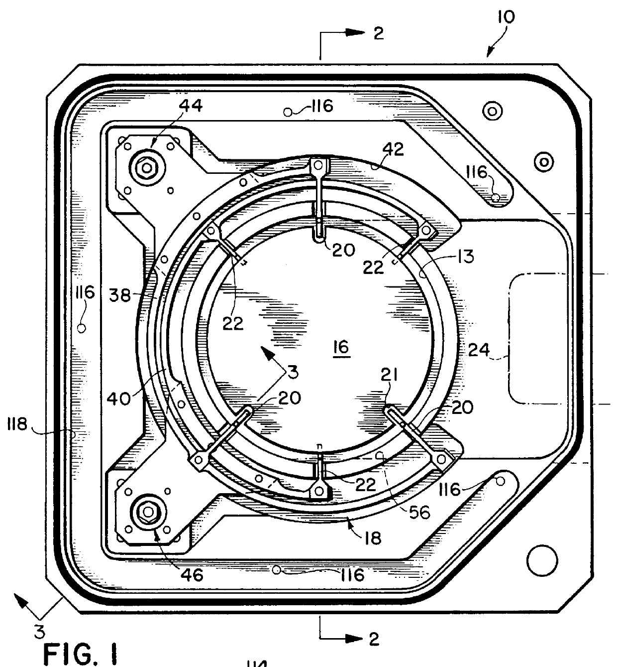
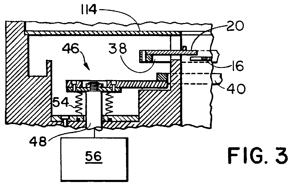
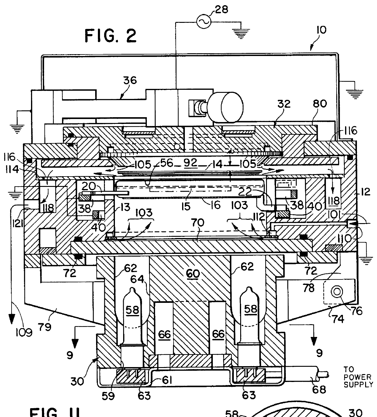
FIGS. 1 and 2 are, respectively, a top plan view of the preferred embodiment of the single wafer, reactor 10 of our present invention, shown with the cover pivoted open, and a vertical cross-section of the reactor 10.

Referring primarily to these two figures and to others indicated parenthetically, the reactor system 10 comprises a housing 12 (also termed a "chamber"), typically made of aluminum, which defines an inner vacuum chamber 13 that has a plasma processing region 14 (FIG. 6). The reactor system 10 also includes a wafer-holding susceptor 16 and a unique wafer transport system 18 (FIG. 1) that includes vertically movable wafer support fingers 20 and susceptor support fingers 22. These fingers cooperate with an external robotic blade 24 (FIG. 1) for introducing wafers 15 into the process legion or chamber 14 and depositing the wafers 15 on the susceptor 16 for processing, then removing the wafers 15 from the susceptor 16 and t...


PUM

PropertyMeasurementUnit
total pressureaaaaaaaaaa
chamber pressureaaaaaaaaaa
pressureaaaaaaaaaa

Abstract

A high pressure, high throughput, single wafer, semiconductor processing reactor is disclosed which is capable of thermal CVD, plasma-enhanced CVD, plasma-assisted etchback, plasma self-cleaning, and deposition topography modification by sputtering, either separately or as part of in-situ multiple step processing. The reactor includes cooperating arrays of interdigitated susceptor and wafer support fingers which collectively remove the wafer from a robot transfer blade and position the wafer with variable, controlled, close parallel spacing between the wafer and the chamber gas inlet manifold, then return the wafer to the blade. A combined RF/gas feed-through device protects against process gas leaks and applies RF energy to the gas inlet manifold without internal breakdown or deposition of the gas. The gas inlet manifold is adapted for providing uniform gas flow over the wafer. Temperature-controlled internal and external manifold surfaces suppress condensation, premature reactions and decomposition and deposition on the external surface. The reactor also incorporates a uniform radial pumping gas system which enables uniform reactant gas flow across the wafer and directs purge gas flow downwardly and upwardly toward the periphery of the wafer for sweeping exhaust gases radially away from the wafer to prevent deposition outside the wafer and keep the chamber clean. The reactor provides uniform processing over a wide range of pressures including very high pressures. A low temperature CVD process for forming a highly conformal layer of silicon dioxide is also disclosed. The process uses very high chamber pressure and low temperature, and TEOS and ozone reactants. The low temperature CVD silicon dioxide deposition step is particularly useful for planarizing underlying stepped dielectric layers, either alone or in conjunction with a subsequent isotropic etch. A preferred in-situ multiple-step process for forming a planarized silicon dioxide layer uses (1) high rate silicon dioxide deposition at a low temperature and high pressure followed by (2) the deposition of the conformal silicon dioxide layer also at high pressure and low temperature, followed by (3) a high rate isotropic etch, preferably at low temperature and high pressure in the sane reactor used for the two oxide deposition steps. Various combinations of the steps are disclosed for different applications, as is a preferred reactor self-cleaning step.

Description

BACKGROUND OF THE INVENTIONThe present invention relates to a reactor and methods for performing single and in-situ multiple integrated circuit processing steps, including thermal CVD, plasma-enhanced chemical vapor deposition (PECVD), reactor self-cleaning, film etchback, and modification of profile or other film property by sputtering. The present invention also relates to a process for forming conformal, planar dielectric layers on integrated circuit wafers and to an in-situ multi-step process for forming conformal, planar dielectric layers that are suitable for use as interlevel dielectrics for multi-layer metallization interconnects.I. ReactorThe early gas chemistry deposition reactors that were applied to semiconductor integrated circuit fabrication used relatively high temperature, thermally-activated chemistry to deposit from a gas onto a heated substrate. Such chemical vapor deposition of a solid onto a surface involves a heterogeneous surface reaction of gaseous species th...

Claims


Application Information

Patent Timeline
Patent Type & Authority Patents(United States)
IPC IPC(8): C23C16/40C23C16/54C23C16/50C23C16/509C23C16/455C23C16/44H01L21/314H01L21/316
CPCC23C16/402C23C16/455C23C16/45521C23C16/45565C23C16/5096C23C16/54H01J37/32082H01J37/3244H01L21/31604H01L21/02164H01L21/02274H01L21/02211
Inventor WANG, DAVID NIN-KOUWHITE, JOHN M.LAW, KAM S.LEUNG, CISSYUMOTOY, SALVADOR P.COLLINS, KENNETH S.ADAMIK, JOHN A.PERLOV, ILYAMAYDAN, DAN
Owner APPLIED MATERIALS INC
Why Eureka
Try Eureka