Thin film transistor array substrate for a liquid crystal display

a technology of thin film transistors and liquid crystal displays, applied in non-linear optics, identification means, instruments, etc., can solve the problems of contact failure, reduced aperture ratio, complicated processing steps, etc., and achieve good performance and reduce the number of masks

Inactive Publication Date: 2008-03-25
SAMSUNG DISPLAY CO LTD
View PDF4 Cites 13 Cited by
  • Summary
  • Abstract
  • Description
  • Claims
  • Application Information

AI Technical Summary

Benefits of technology

[0009]It is an object of the present invention to provide a TFT array substrate for a liquid crysta

Problems solved by technology

In photolithography, many masks should be used for uniformly etching the thin films, and this involves complicated processing steps and increased production cost.

Method used


Image

  • Thin film transistor array substrate for a liquid crystal display
  • Thin film transistor array substrate for a liquid crystal display
  • Thin film transistor array substrate for a liquid crystal display

Examples


first preferred embodiment

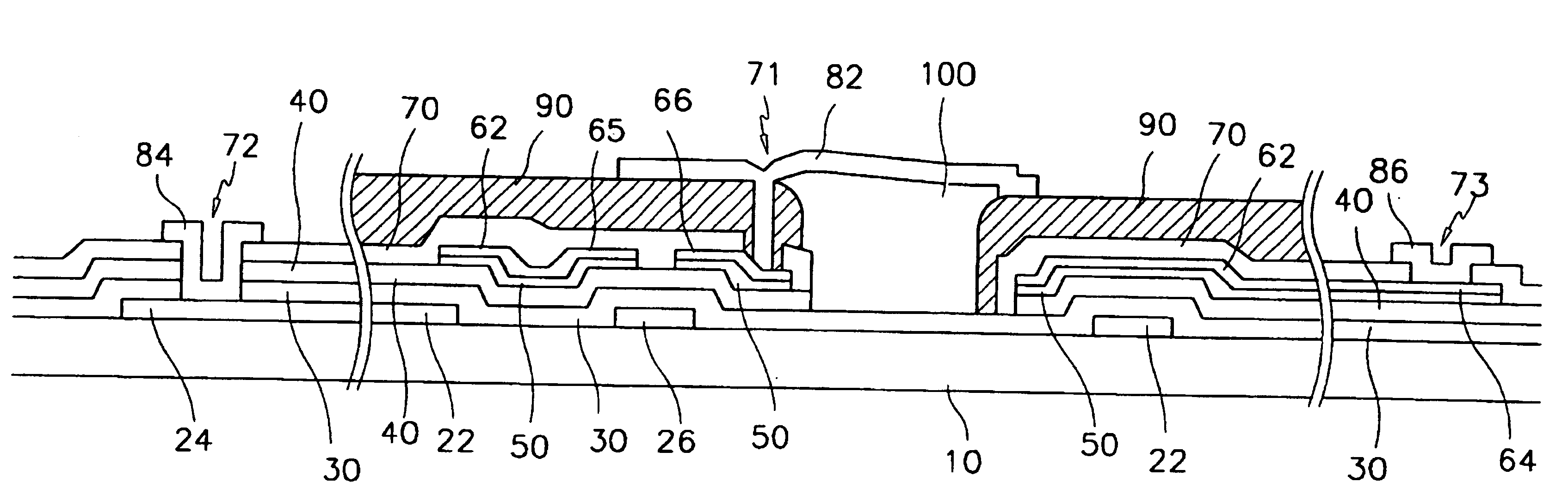
[0084]FIGS. 1 to 5 illustrate a TFT array substrate according to a first preferred embodiment of the present invention.

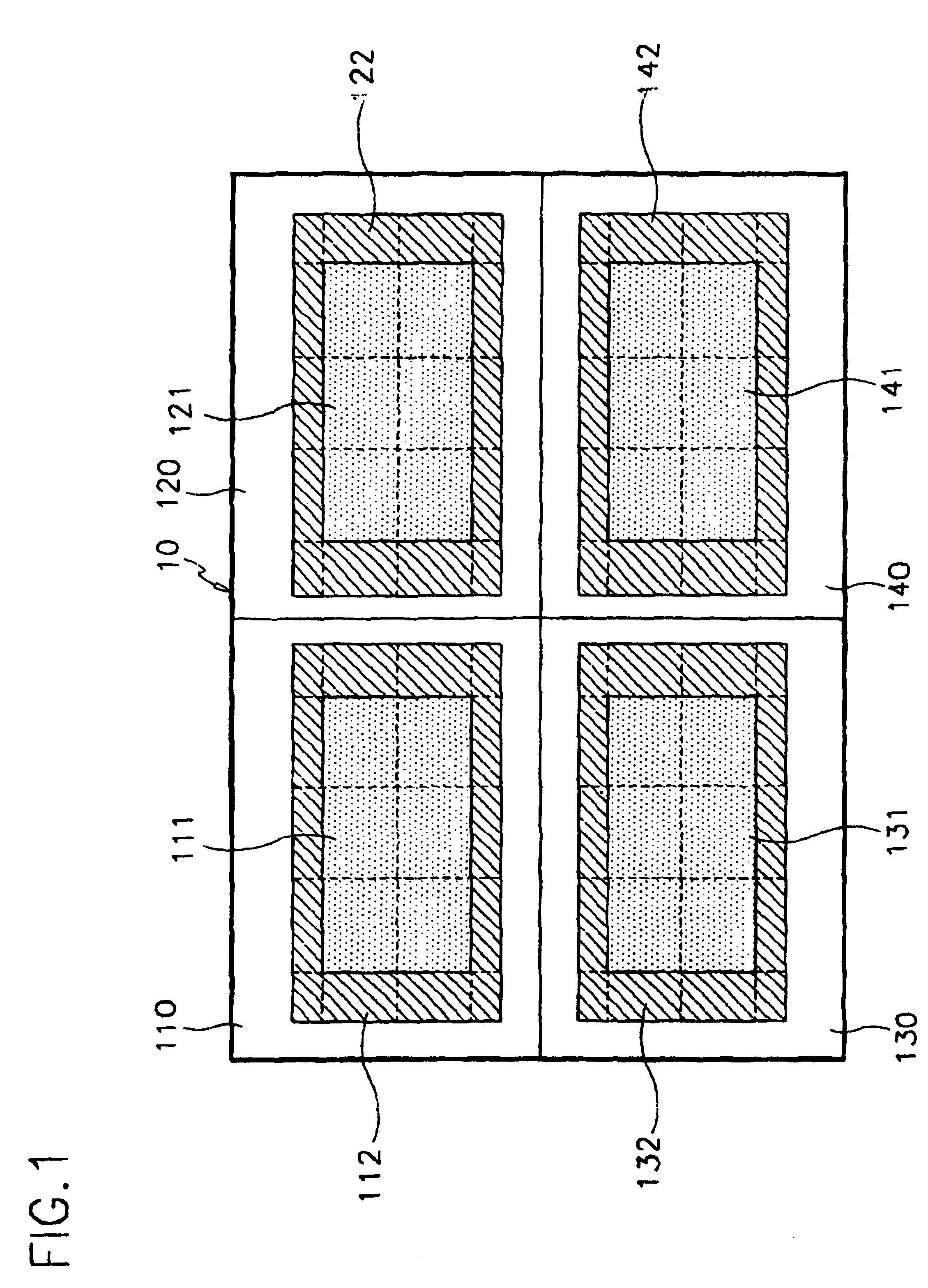
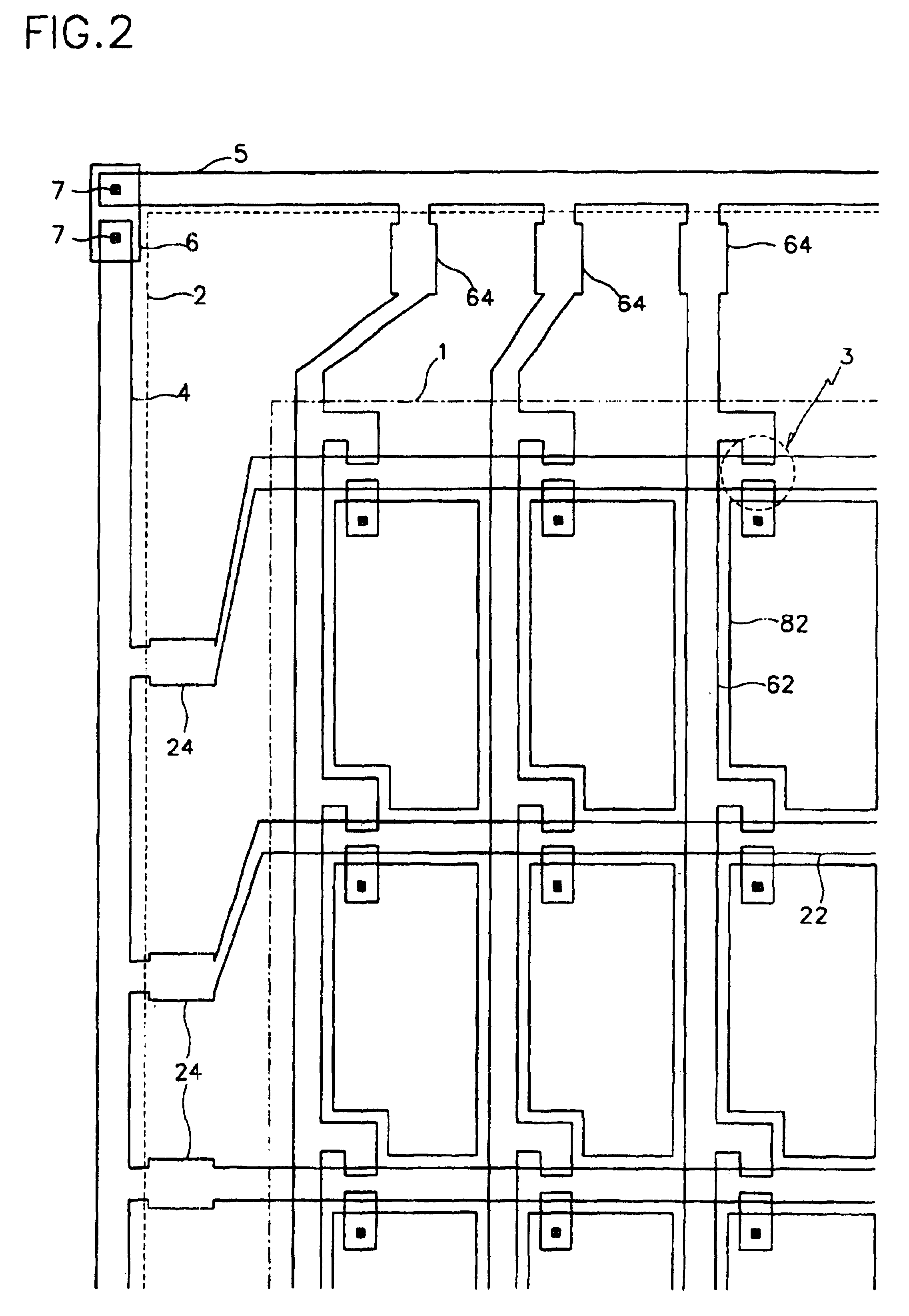
[0085]A plurality of panel regions for LCDs may be made at one insulating substrate at the same time. For example, as shown in FIG. 1, four panel regions 110, 120, 130 and 140 are made with display areas 111, 121, 131 and 141, and peripheral areas 112, 122, 132 and 142. TFTs, lines and pixel electrodes for the main components are repeatedly arranged at the display areas 111 to 141, whereas pads and other static electricity protection circuits for the components connected to the driving circuits are provided at the peripheral areas 112 to 142.

[0086]The display areas 111 to 141 and the peripheral areas 112 to 142 are divided into several regions, and each region is light-exposed by a stepper. A photoresist film coated the substrate is exposed to light using identical or different masks per region. After the exposure, the photoresist film is wholly developed to form a ...

second preferred embodiment

[0138]FIGS. 18 to 23 illustrate a method for fabricating a TFT array substrate according to a second preferred embodiment of the present invention. In this preferred embodiment, the processing steps are the same as those related to the first preferred embodiment up to the step of depositing the passivation layer 70 onto the substrate 10.

[0139]As shown in FIG. 18, a photoresist film PR is coated onto the passivation layer 70. The photoresist film PR is exposed to light through a third mask, and developed to form a photoresist pattern. That is, the portion B of the photoresist film PR over the gate pad 24, data pad 64 and drain electrode 66 is completely removed. The portion C of the photoresist film PR adjacent to the portion B over the drain electrode 66 and the data pad 64 and positioning at the pixel area is partially removed such that it has a small thickness. The remaining portion A of the photoresist film PR is left without being consumed.

[0140]Thereafter, as shown in FIG. 19, ...

third preferred embodiment

[0148]FIGS. 24 to 29 illustrate the steps of fabricating a TFT array substrate according to a third preferred embodiment of the present invention where a photosensitive organic layer is used for the passivation layer. In this preferred embodiment, the processing steps are similar to those related to the first preferred embodiment prior to the step of depositing a passivation layer onto the substrate 10.

[0149]As shown in FIG. 24, a photosensitive passivation layer 80 of a photosensitive organic material is deposited onto the substrate 10 to a thickness of 3,000 Å. The photosensitive passivation layer 80 is then exposed to light through a third mask, and developed to form a photoresist pattern. That is, the portion B of the photosensitive passivation layer 80 over the gate pad 24, the data pad 64 and the drain electrode 66 is completely removed. The portion C of the photosensitive passivation layer 80 adjacent to the portion B over the drain electrode 66 and the data pad 64 and positi...


PUM


Abstract

A thin film transistor substrate for a liquid crystal display includes an insulating substrate, and a gate line assembly formed on the substrate. The gate line assembly has a double-layered structure with a lower layer exhibiting good contact characteristics with respect to indium tin oxide, and an upper layer exhibiting low resistance characteristics. A gate insulating layer, a semiconductor layer, a contact layer, and first and second data line layers are sequentially deposited onto the substrate with the gate line assembly. The first and second data line layers are patterned to form a data line assembly, and the contact layer is etched through the pattern of the data line assembly such that the contact layer has the same pattern as the data line assembly. A passivation layer is deposited onto the data line assembly, and a photoresist pattern is formed on the passivation layer by using a mask of different light transmissties mainly at a display area and a peripheral area. The passivation layer and the underlying layers are etched through the photoresist pattern to form a semiconductor pattern and contact windows. A pixel electrode, a supplemental gate pad and a supplemental data pad are then formed of indium tin oxide or indium zinc oxide. The gate and data line assemblies may be formed with a single layered structure. A black matrix and a color filter may be formed at the structured substrate before forming the pixel electrode, and an opening portion may be formed between the pixel electrode and the data line to prevent possible short circuits.

Description

BACKGROUND OF THE INVENTION[0001](a) Field of the Invention[0002]The present invention relates to a thin film transistor array (TFT) substrate for a liquid crystal display and a method for fabricating the same, and more particularly, to a method for fabricating a TFT array substrate of good performance in processing steps.[0003](b) Description of the Related Art[0004]Generally, a liquid crystal display (LCD) is formed with two glass substrates, and a liquid crystal layer sandwiched between the substrates.[0005]One of the substrates has a common electrode, a color filter and a black matrix, and the other substrate has pixel electrodes and thin film transistors (TFTs). The former substrate is usually called the “color filter substrate,” and the latter substrate is usually called the “TFT array substrate.”[0006]The TFT array substrate is fabricated by forming a plurality of thin films on a glass substrate, and performing photolithography with respect to the thin films. In photolithogra...

Claims


Application Information

Patent Timeline
IPC IPC(8): H01L29/04G02F1/136G02F1/1333G02F1/1335G02F1/1362G02F1/1368G09F9/00G09F9/30H01L21/336H01L21/77H01L21/84H01L27/12H01L29/45H01L29/49H01L29/786
CPCG02F1/13458G02F1/136286H01L27/1288H01L29/458H01L29/4908H01L27/124G02F2001/136222G02F2001/136231G02F2201/40G02F2001/13629G02F1/136222G02F1/136231G02F1/13629
Inventor PARK, WOON-YONGYOON, JONG-SOOJEONG, CHANG-OH
Owner SAMSUNG DISPLAY CO LTD
Why Eureka
Try Eureka