Carbon tube nanometer tube figuring technique

A technology of carbon nanotubes and process methods, which can be applied in nanotechnology, nanotechnology, nanostructure manufacturing, etc., and can solve problems such as low efficiency and limitations

Inactive Publication Date: 2009-03-18
TSINGHUA UNIV
View PDF5 Cites 0 Cited by
  • Summary
  • Abstract
  • Description
  • Claims
  • Application Information

AI Technical Summary

Problems solved by technology

[0003] The construction of electronic devices based on carbon nanotubes requires a method to control the positioning of carbon nanotubes. At present, some people use AFM to manipulate the positioning of carbon nanotubes, but the efficiency is very low. Another method is to make carbon nanotubes on a patterned catalyst. Growth, because the growth of carbon nanotubes generally requires a very high temperature, which has great limitations on the substrate. The published patent No. 1502553 is to grow carbon nanotubes on a patterned substrate

Method used


Image

  • Carbon tube nanometer tube figuring technique
  • Carbon tube nanometer tube figuring technique
  • Carbon tube nanometer tube figuring technique

Examples


Embodiment 1

[0030] Patterned deposition of carbon nanotubes on silicon substrates:

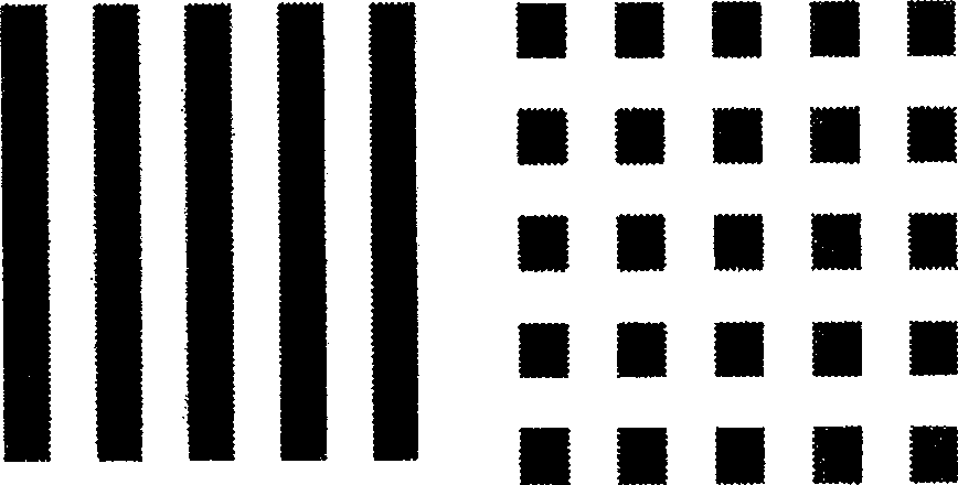
[0031] A single crystal silicon wafer N(100) is used as the substrate, and a layer of Megaposit SPR6112B photoresist is coated on it, and the photoresist is exposed according to the pre-designed stripes and dot patterns of different sizes. After exposure and development, the exposed silicon wafer is exposed. The OTS methyl surface self-assembly film was partially assembled, and then soaked in acetone to remove the remaining photoresist, and then the APTES amino surface self-assembly film was assembled on the silicon wafer after removal. In this way, a patterned self-assembled film surface (such as figure 1 shown).

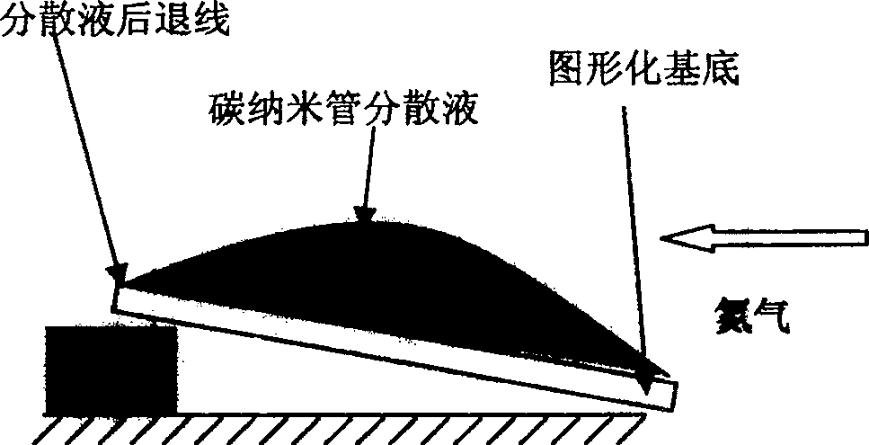
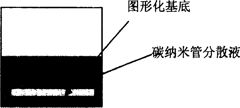
[0032] The patterned functionally treated silicon substrates were immersed in SDS aqueous solution or DMF carbon nanotube dispersions (e.g. image 3 shown) for 16 hours, after taking out, rinse with deionized water or anhydrous methanol, respectively, and dry with nitrogen.

Embodiment 2

[0034] Patterned deposition of carbon nanotubes on electrode aluminum substrates:

[0035] A single crystal silicon wafer N(100) is used as the substrate, a layer of Al is sputtered on the cleaned silicon wafer, and then a layer of Megaposit SPR6112B photoresist is coated on the Al, and stripes and lattice patterns of different sizes are designed in advance. Expose the photoresist, then etch the exposed part of Al (phosphoric acid corrosion), assemble the OTS methyl surface self-assembly film on the silicon wafer part exposed by etching the Al, and then soak it in acetone for the photolithography of the Al surface Glue and degumming, and then assemble the APTES amino surface self-assembled film on top of the degummed Al to form patterns of different surface self-assembled films (such as figure 1 shown).

[0036] The patterned substrate was immersed in SDS aqueous solution or DMF carbon nanotube dispersion for 16 hours, then taken out and washed with deionized water or anhydro...

Embodiment 3

[0038] A patterned carbon nanotube film is obtained by a patterned casting process of carbon nanotubes on an aluminum electrode substrate.

[0039] A single crystal silicon wafer N(100) is used as the substrate, a layer of Al is sputtered on the cleaned silicon wafer, and then a layer of Megaposit SPR6112B photoresist is applied on the Al, and stripes and lattice patterns of different sizes designed by oneself are used. Expose the photoresist, then etch the Al in the exposed part, assemble the OTS methyl surface self-assembly film on the silicon wafer exposed by etching the Al, and then soak it in acetone to remove the photoresist on the Al surface, Hydroxylated again to form a hydrophobic OTS film and a pattern of hydrophilic aluminum (e.g. figure 1 shown).


PUM

PropertyMeasurementUnit
diameteraaaaaaaaaa
diameteraaaaaaaaaa

Abstract

The invention discloses a process for graph carbon nanometer tube, belongs to field of nanometer science and technology. The said means mainly uses the force of functionalization organosilane self assembling monolayer film surface force to the carbon nanometer tube in the DMF and the SDS dispersion to graph the single, multilayer film or array of the carbon nanometer tube. Forming graph on the surface in photoetching process, and then assembling different self assembly film on the different surface or area of the gragh, forming single-layer or multilayer construction graph carbon nanometer tube in precipitation and casting art work using the nature of different area and different surface of the graph film. The means can easily form carbon nanometer tube graph on glass, silicon chip or plastic, and also can form carbon nanometer tube array graph on aluminium and other metal. The invention is provided with latent application value in artwork of making panel display screen, transistor, and chemical and biology sensor and semiconductor device.

Description

technical field [0001] The invention relates to a carbon nanotube patterning process method based on a self-assembled film, which is widely used in micro-nano manufacturing, and belongs to the field of nanometer science and technology. Background technique [0002] In 1991, Iijima of Japan first discovered multi-walled carbon nanotubes (MWNTs) with a diameter of 4-30nm and a length of 1um. In 1993, single-walled carbon nanotubes (SWNTs) were also discovered, with diameters ranging from 0.4 nm to 3-4 nm and lengths up to several micrometers. Carbon nanotubes have unique electronic, mechanical and chemical properties, and have a wide range of applications in the fields of machinery, electrochemistry, energy, and display devices. Carbon nanotubes have two unique and excellent electrical properties, one is the field emission property, and the other is the dual electrical properties of carbon nanotubes. These two unique electrical properties make this new material promising for...

Claims


Application Information

Patent Timeline
Patent Type & Authority Patents(China)
IPC IPC(8): B82B3/00C01B31/02
Inventor 胡元中彭倚天王慧
Owner TSINGHUA UNIV
Why Eureka
Try Eureka