
A method for making GaMnN sparse magnetic semiconductor nano wire

A technology of dilute magnetic semiconductors and nanowires, applied in semiconductor/solid-state device manufacturing, electrical components, circuits, etc., can solve problems such as the influence of magnetic properties of materials, difficult materials, and low sample output

Inactive Publication Date: 2009-11-04
PEKING UNIV
View PDF3 Cites 1 Cited by
  • Summary
  • Abstract
  • Description
  • Claims
  • Application Information

AI Technical Summary

Problems solved by technology

However, due to the low solid solubility of magnetic ions in semiconductors, it is still very difficult to prepare highly doped GaMnN dilute magnetic semiconductor materials with Mn replacing lattice cations by traditional methods. Moreover, it has been reported in the literature that using the above method If the doping concentration of Mn in GaN is greater than 3at.% during preparation, Mn ions will fill in the lattice gap instead of replacing Ga, thus forming Ga x mn y Crystal grains affect the magnetic properties of the material, and there is a problem of magnetic impurity phase precipitation
People such as Deepak (F.L.Deepak, P.U.Vanitha, A.Fovindaraj, C.N.R.Rao, Chem.Phys.Lett.374 (2003) 314) utilize carbon nanotube as template, have prepared GaMnN dilute magnetic semiconductor nanowire, but sample yield is relatively low few

Method used


Image

  • A method for making GaMnN sparse magnetic semiconductor nano wire
  • A method for making GaMnN sparse magnetic semiconductor nano wire
  • A method for making GaMnN sparse magnetic semiconductor nano wire

Examples


Embodiment 1

[0019] 1. GaMnN dilute magnetic semiconductor nanowires were prepared in large quantities by oxide ammoniation method.

[0020] A Si sheet coated with a 5nm gold film was used as the collection substrate of the product, and the MnCl 2 4H 2 A small ceramic cup of O powder, a gallium source substrate (a Si sheet with 100 mg of gallium metal placed on it) and three collection substrates were put into a quartz boat with one end open in turn, and the small ceramic cup was about 10 cm away from the gallium source substrate. Then place the quartz boat in the center of the tube furnace with the open end facing the direction of the airflow. After closing the system, turn on the mechanical pump to evacuate to a vacuum, pass in argon gas for cleaning, and raise the system pressure to normal pressure, and repeat this three times. After the experiment started, the required pressure (0.6-0.9 standard atmospheric pressure) was maintained by manually controlling the needle valve, and the he...


PUM

PropertyMeasurementUnit
diameteraaaaaaaaaa

Abstract

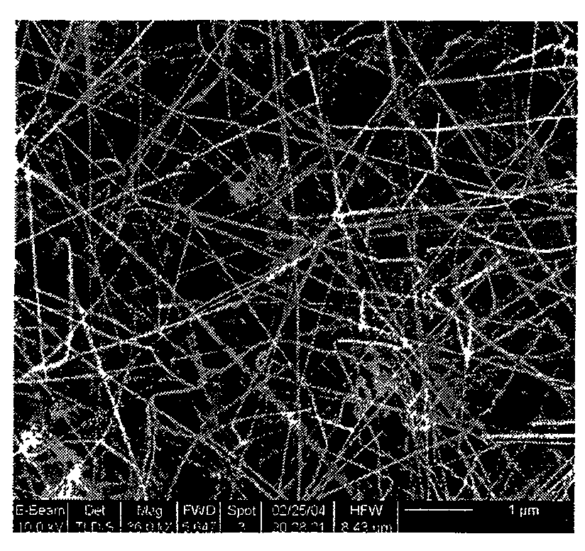
The invention discloses a method for preparing GaMnN dilute magnetic semiconductor nanowires. The method of the present invention comprises the following steps: 1) Mn doping: in-situ doping Mn on Ga2O3 nanowires; 2) ammoniation: ammoniating Ga2O3 nanowires doped with Mn under an ammonia atmosphere to obtain GaMnN dilute Magnetic semiconductor nanowires. The method of the invention is simple and requires less equipment, the prepared GaMnN nanowire has strong ferromagnetism, the Curie temperature is higher than room temperature, and its magnetic doping concentration is controllable, the nanowire has high purity, large output, and linear shape control (adjustment of growth parameters such as air pressure can prepare nanowires with a diameter of tens of nanometers to hundreds of nanometers), and can be used for spin field effect transistors (spin-FETs), spin light-emitting diodes (spin-LEDs), and spin resonance The fabrication of nano-spintronic devices such as spin-RTD has broad application prospects.

Description

technical field [0001] The invention relates to a method for preparing nanowires, in particular to a method for preparing GaMnN dilute magnetic semiconductor nanowires. Background technique [0002] The room temperature ferromagnetism of dilute magnetic semiconductor materials is an important property of whether it can be used in the manufacture of spintronic devices. As a wide bandgap semiconductor material, GaN has excellent optical and electrical properties. In theory, GaN doped with Mn will make It has a ferromagnetic order higher than room temperature, so GaMnN dilute magnetic semiconductor materials are current research hotspots. However, due to the low solid solubility of magnetic ions in semiconductors, it is still very difficult to prepare highly doped GaMnN dilute magnetic semiconductor materials with Mn replacing lattice cations by traditional methods. Moreover, it has been reported in the literature that using the above method If the doping concentration of Mn i...

Claims


Application Information

Patent Timeline
Patent Type & Authority Patents(China)
IPC IPC(8): H01L21/18
Inventor 俞大鹏宋祎璞王朋伟
Owner PEKING UNIV
Learn More