Surface treatment method for copper and copper

A surface treatment, copper surface technology, applied in the direction of metal material coating process, etc., can solve the problems of reducing insulation reliability, insulation reliability, short circuit, etc., to achieve the effect of ensuring bonding strength and improving reliability

Active Publication Date: 2008-03-05
株式会社力森诺科
View PDF5 Cites 24 Cited by
  • Summary
  • Abstract
  • Description
  • Claims
  • Application Information

AI Technical Summary

Problems solved by technology

However, in the formation of fine wiring, the unevenness of the copper surface that is in close contact with the resist becomes needle-like, and similar to the above, due to the residue of the resist, there is a problem of short-circuiting between the wirings, and it is impossible to obtain a good bond between the copper surface and the insulating resin. Or the problem of the adhesion between the copper surface and the solder resist, the problem of non-precipitation of gold plating or uneven gold plating
[0018] In addition, in the formation of fine wiring by the semi-additive method, unevenness can be formed on the copper seed layer formed by sputtering. However, similar to the above, since the resist cannot be completely removed from the copper surface, there may be unevenness in the seed layer. Difficulty in forming wiring on the surface, short circuit between wiring, inability to obtain adhesion between copper surface and insulating resin or copper surface and solder resist, non-deposited gold plating or uneven gold plating
[0019] In addition, the height variation of unevenness becomes large. If Rz1.0μm, there will be a transmission loss similar to the first conventional technology. big problem
In addition, because the needle-like crystals of copper oxide are easily damaged, it is impossible to perform horizontal line processing, and there is a problem of poor operability when processing thin plates
In addition, in the plating process of through-hole connection, since the needle-shaped crystals of copper oxide are dissolved, pink circles (pink circles) are formed around the through-holes, and insulation reliability is reduced in parts where the insulation distance between wirings is short. Or easy to peel between the copper surface and the insulating resin
In addition, since a high-temperature alkaline solution is used, the surface of the insulating resin is easily invaded, and the insulation reliability is easily reduced due to ion contamination or insulation deterioration
In addition, when washing with water after oxidation treatment, due to the complicated needle-shaped crystal irregularities of copper oxide, water washing between the needle-shaped crystals cannot be sufficiently performed, and there is a problem that the insulation reliability is likely to be lowered due to residual ions between the crystals.
[0020] The third conventional technique is to provide fine needle-like crystals of metallic copper on the copper surface to improve the bonding strength between the copper surface and the resist or between the copper surface and the insulating resin, because there is no The needle-shaped crystals of metallic copper are dissolved, so no pink circles are generated. However, similar to the second prior art, in the formation of fine wiring, short circuits between wirings may occur due to the residue of the resist. The problem is that the adhesion between the copper surface and the insulating resin or the copper surface and the solder resist cannot be obtained, the problem of non-precipitation of gold plating or uneven gold plating occurs, and the problem of reduced bonding reliability at high temperature and high humidity, Problems of increased transmission loss, problems of poor operability when handling thin plates, problems of reduced insulation reliability due to ion contamination or insulation deterioration of insulating materials, problems of reduced insulation reliability due to water washability after oxidation treatment

Method used


Image

  • Surface treatment method for copper and copper
  • Surface treatment method for copper and copper
  • Surface treatment method for copper and copper

Examples


Embodiment approach

[0148] [Example]

[0149] Hereinafter, the present invention will be described in detail based on examples, but the present invention is not limited thereto.

Embodiment 1

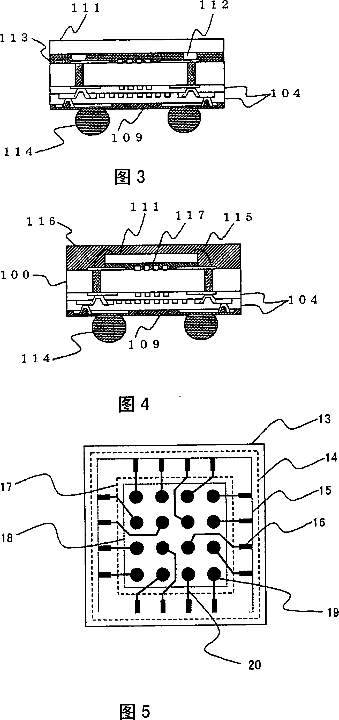
[0151] In order to evaluate the reliability of the semiconductor package produced using the copper surface treatment of the present invention, a semiconductor package sample was produced by the following method.
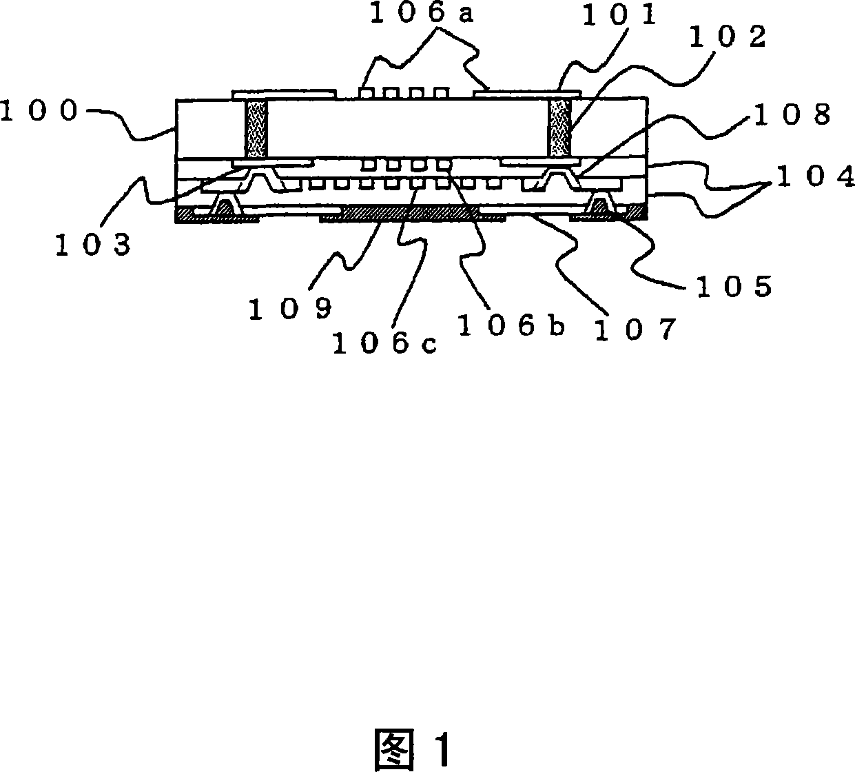
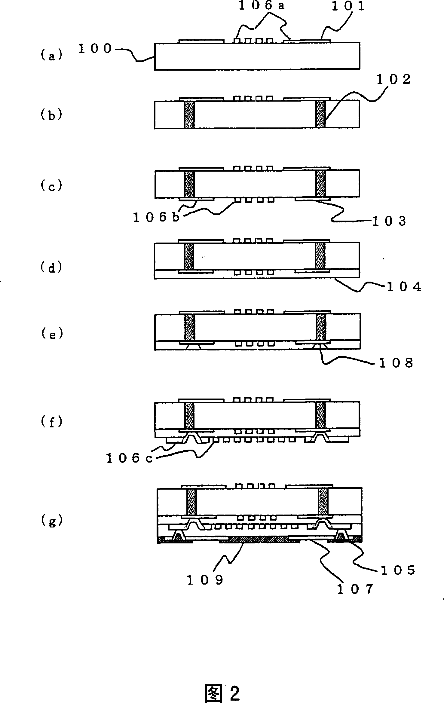
[0152] (Process a)

[0153] Prepare a 0.4mm thick soda lime glass substrate (thermal expansion coefficient 11ppm / °C) as the core substrate 100, form a 200nm copper thin film on one surface by sputtering, then electroplate with copper to a thickness of 10μm, and then sputter The irradiation was carried out using an apparatus model MLH-6315 manufactured by Nippon Vacuum Technology Co., Ltd., under Condition 1 described below.

[0154] Condition 1

[0155] Current: 3.5A

[0156] Voltage: 500V

[0157] Argon flow: 35SCCM (0.059Pa m 3 / s)

[0158] Pressure: 5×10 -3 Torr (6.6×10 -1 Pa)

[0159] Film forming speed: 5nm / sec

[0160] Then, an etch resist is formed on the portion to be the first wiring 106a, etched using a ferric chloride etching solution to remove th...

Embodiment 2

[0197] In addition to forming copper oxide crystals on the surface of the second wiring 106b in (step d-2), before forming the build-up layer 104 in (step d-3), wash the surface of the second wiring 106b with water for 5 minutes In addition to the reduction treatment process of immersing in the reduction treatment solution HIST-100D (manufactured by Hitachi Chemical Industry Co., Ltd., trade name) at 40°C for 3 minutes, washing with water for 10 minutes, and drying at 85°C for 30 minutes, the remaining In the same manner as in Example 1, a substrate for mounting a semiconductor chip for a fan-in BGA and a semiconductor package were produced.


PUM

PropertyMeasurementUnit
surface roughnessaaaaaaaaaa

Abstract

A copper surface treatment method is provided to ensure adhesive strength between a copper surface and an insulating layer without forming a recess and a protrusion over 1[mu]m due to copper surface treatment and to improve insulation reliability between wirings. A copper is also provided. The surface treatment method is provided with a step of discretely forming a metal nobler than copper on the copper surface, and a step of successively oxidizing the copper surface by an alkaline solution including an oxidizing agent. The copper whose surface is treated by such method is also provided.

Description

technical field [0001] The present invention relates to a copper surface treatment method and copper surface-treated by the surface treatment method. Background technique [0002] In recent years, the development of the information society has been astonishing. Computers and mobile phones in consumer equipment are developing towards miniaturization, light weight, high performance, and high functionality. As industrial equipment, wireless base stations, optical communication devices, servers, Network-related equipment such as routers, etc., regardless of large or small, also seek to improve their functions. In addition, with the increase in the amount of information transmitted, the signal to be processed tends to increase in frequency every year. High-speed processing and high-speed The development of transmission technologies is actively underway. Regarding the mounting relationship, at the same time, we are actively promoting the high-speed and high-functionalization of L...

Claims


Application Information

Patent Timeline
Patent Type & Authority Applications(China)
IPC IPC(8): C23C22/78C23C22/63C23C22/83
Inventor 山下智章井上康雄松浦雅晴伊藤丰树清水明井上文男中祖昭士
Owner 株式会社力森诺科
Why Eureka
Try Eureka